
Performance characteristics and application analysis of LVDS ultra-high-speed crosspoint switch SCAN90CP02
“LVDS has been widely used in interface devices and field programmable gate arrays (FPGA), application specific integrated circuits (ASIC), and the systems using LVDS have successfully achieved high-speed interconnection. Then, not all LVDS I/O interfaces have good performance. For example, the LVDS I/O of some ASICs or FPGAs may not be as suitable for driving differential traces on a PCB as the LVDS I/O in standard devices.
“
Authors: Xu Mengxiang, Yang Fei, Zhang Eryang
introduction
LVDS has been widely used in interface devices and field programmable gate arrays (FPGA), application-specific integrated circuits (ASIC), and the systems using LVDS have successfully achieved high-speed interconnection. Then, not all LVDS I/O interfaces have good performance. For example, the LVDS I/O of some ASICs or FPGAs may not be as suitable for driving differential traces on a PCB as the LVDS I/O in standard devices. Even well-designed standard devices have poor signal transmission quality due to PCB layout problems. When using ASIC or FPGA as the core part of the system, it is sometimes impossible to place the device as close as possible to the connector, which will cause the trace to change, the reflection to increase, and the loss to increase. In order to eliminate the problems existing in the interconnect, National semiconductor has introduced a series of small size buffers. This article will introduce the function and application of its LVDS ultra-high-speed cross-point switch SCAN90CP02.
1 Introduction to SCAN90CP02
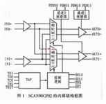
The SCAN90CP02 circuit is a 1.5Gb/s 2×2 low-voltage differential signal transmission analog crosspoint switch introduced by National Semiconductor. Its high-speed data path and flow-through pins minimize jitter within the circuit. Its configurable pre-enhancement function (0/25/50/100% selectable) overcomes the effects of external ISI (Inter Symbol Interference) jitter when signals are transmitted over lossy backplanes and cables. Its differential inputs can be connected to LVDS and Bus LVDS signals, as well as to signal levels such as Common Mode Logic (CML) and Low Voltage Positive Emitter Coupled Logic (LVPCL). The SCAN90CP02 uses a non-block crosspoint structure and can be configured as a 1:2 clock or data distributor, 2:1 redundant multiplexer, crossover function, and double buffers for signal enhancement and stub hiding. Figure 1 is the internal block diagram of SCAN90CP02.
The integrated IEEE 1149.1 (JTAG) and 1149.6 test input circuit TAP (Test Access Port) of SCAN90CP02 supports the testability of single-ended LVTTL/CMOS and differential LVDS PCB interconnection. These capabilities help reduce test time and reduce test and development costs. The circuit uses a 3.3V power supply, CMOS process and LVDS I/O, ensuring high performance and low power consumption over the entire industrial temperature range (-40°C to +85°C).
The SCAN90CP02 can truly eliminate jitter, thereby improving system reliability and enabling users to interconnect with lower-cost lines. Because the SCAN90CP02 has a pre-enhancement function, it can not only perform normal switching functions, but also can be used as a buffer to amplify the LVDS signals of existing FPGAs, ASICs, and serial/deserializers (SerDes). In addition, the LVDS output of this circuit does not support a multidrop BLVDS environment.
The features of SCAN90CP02 are as follows:
●The transmission rate of each channel reaches 1.5Gb/s.
●Low power consumption, in dual repeater mode, the current at the highest rate is only 70mA.
●Low output jitter.
● Configurable pre-enhancement (0/25/50/100%) to drive lossy backplanes and cables.
●Have through (Flow-through) pin lead-out.
●LVDS/BLVDS/CML/LVPECL input, LVDS output.
●Apply to IEEE 1149.1 and 1149.6 standards.
●Single power supply 3.3V power supply.
●The input and output can be controlled separately to reduce power consumption.
●Industrial temperature range (-40℃ to ±85℃).
The SCAN90CP02 is available in a 28-pin LLP package or a 32-pin LQFP package.
The pre-enhancement function of the circuit is used to compensate for long distance transmission or lossy transmission medium. To minimize power dissipation, the circuit provides separate pins for each output. And the pre-increment function is a programmable device.
2 Application of SCAN90CP02
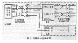
In the author’s design project, it is necessary to transmit data at a rate of up to 600Mb/s, and the transmitter and receiver complete tasks such as data transceiver, modulation and channel matching. In order to test the quality of the data transmission of the whole communication system, the author also designed a high-speed bit error rate tester. The tester consists of 3 circuit boards, which are the clock generating board, the sending board and the receiving board. A SCAN90CP02 is used on the clock generation board and the hair board. One is to make the output signal on the circuit board as close to the connector as possible, to reduce the wiring pressure of the core circuit on the board, and to make the placement more free; the other is to complete the electrical The level conversion task is to convert the LVPECL level to the LVDS level; the third is to compensate the loss of the wiring to ensure that the signal has better transmission quality. The block diagram of the bit error tester is shown in Figure 2, in which the connection mode of the SCAN90CP02 is highlighted. The various boards in this tester are described in detail below.
(1) Clock board. The SCAN90CP02 of the clock board is configured as a 1:2 splitter, and EN0, EN1, SEL0 and SEL1 are all set to low level. The 300MHz clock signal generated by the clock board is LVPECL level, which is converted into 2-way LVDS level by SCAN90CP02, and sent to the sending board and the receiving board of the bit error tester respectively.
(2) Hair board. The board is based on the VirtexII series XC2V250 circuit of Xilinx Company as the core, which is composed of some peripheral circuits and control circuits, and completes functions such as pseudocode generation, data framing, and parallel-serial conversion. The output 600Mb/s data and 300MHz clock are interrupted by SCAN90CP02 and sent to the transmitter through the connector. SCAN90CP02 is configured as a dual-channel interrupter mode, SEL1 is set to high level, and other control terminals are set to level.
(3) Close the board. The closing board takes the VirtexII series XC2V250 circuit of Xilinx Company as the core, and is composed of some peripheral circuits and control circuits. Realize the functions of frame synchronization, data recovery, serial-to-parallel conversion, comparison count and error statistics Display.
The pre-enhancement control terminal of SCAN90CP02 adopts the DIP switch to select high and low level to increase the flexibility of design.
3 Conclusion
In many applications, especially when connected with high-loss backplanes and cables, the driving capability of some circuits (such as ASIC and FPGA, etc.) is often insufficient, which requires the use of circuits with pre-enhancement functions (such as SCAN90CP02). Amplification, which can not only ensure that the receiver obtains sufficient input signal voltage, but also increase the transmission distance and improve the signal quality. Especially when the LVDS transmission method is adopted, its anti-interference ability is greatly enhanced, and the electromagnetic radiation is also reduced.
The Links: LP150E07-A3 SKIIP26AC126V1 IGBT-SUPPLIER


