
“The FS85 series is a functional safety system basis chip (Safety SBC) launched by NXP. Here is an introduction to this chip and its points of attention in hardware design.
“
The FS85 series is a functional safety system basis chip (Safety SBC) launched by NXP. Here is an introduction to this chip and its points of attention in hardware design.
1. Chip introduction
1 Overview
FS85/FS84 is an automotive functional safety multi-output power supply, ranging from radar, vision, ADAS domain controller, radio and infotainment applications. The chip includes switching multiple modes and linear voltage regulators, enhanced safety features and fail-safe outputs. This makes it completely a part of a safety-oriented system, reaching the ASIL D safety integrity level. (The FS84 series is compatible with the FS85 series of chips, and its safety level is ASIL B).
The main performance characteristics are as follows:
• The input voltage up to 60V is suitable for the car and truck market
• Multiple SMPs and LDOs to provide S32 microcontrollers and other more needs
• Standby mode and sleep current is very low (10μA)
• 32-bit SPI and IDC and CRC interface
• Suitable for ASIL D system design with independent safety monitoring device
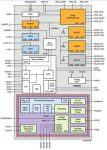
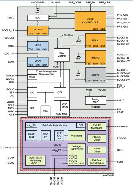
2. The internal block diagram of FS85 is as follows:
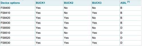
FS85/84 currently includes 4 models, each with different output configurations. This configuration can make it more flexible in the selection of different applications, and thus the total grams of the internal use system. The model table is as follows:
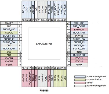
3. Package and pin introduction
The package of PF85 is HPQFN56 (HPQFN56 (SOT684-23) pin package, and its pin package layout is as follows:
4. Unused pin processing method: (Because there are many pin introductions, please refer to Section 8 “Connection of unused pins” of SHEET for detailed information)
The unused pins must be handled strictly in accordance with the description of the manual when designing. as the picture shows:
2. Hardware design guide
1. VPRE
VPRE is a high voltage, synchronous, peak current mode step-down controller. VPRE works in force PWM mode and uses external NMOS. The typical application block diagram is as follows:
The output voltage of VPRE can be set from 3.3V to 5.0V through OTP, its operating frequency is 455 kHz, and the output current reaches a peak value of 10A. VPRE is also the input source of BOOST and BUCK1/2 (it can also be the input source of BUCK3 and LDO1).
When using two FS85/FS84, only one VPRE may be needed. You can optimize the material list without attaching the external components of the second VPRE. At this time, the request of VPRE2 special pin needs to be satisfied:
PRE_FB2 must be connected to PRE_FB1
PRE_CSP2 must be connected to PRE_FB1
PRE_COMP2 must remain open
PRE_SW2 must be connected to GND
PRE_BOOT2 must be connected to VBOS2
PRE_GHS2 and PRE_GLS2 must be left floating
Finally, after the start-up phase is over, VPRE 2 needs to be disabled with the VPDIS bit via SPI/I2C.
2. VBOOST
The VBOOST module is a low voltage, asynchronous, peak current mode boost converter. VBOOST works in PWM mode, using external diodes and internal low-side FETs. The input source of VBOOST must be connected to the output of VPRE.
The typical application block diagram is as follows:
The output voltage of VBOOST can be set from 5.0V to 5.74V through OTP, its operating frequency is 2.22MHz, and the output current is limited to a peak value of 1.5A. The specific output current of the new VPRE is as follows:
When VPRE is configured as 4.1V or 5.0V, VBOOST can be omitted. In the market, you can optimize the list of materials without posting external VBOOST components. The OTP_BOOSTEN bit should be programmed to 0, and the VBOOST pin must be connected to VPRE. The BOOST_LS pin must be left floating.
3. BUCK1 & 2
BUCK1 & 2 blocks are low voltage, synchronous, valley current mode BUCK converters that integrate HS PMOS and LS NMOS. BUCK1 & 2 work in PWM mode, and the output voltage can be set from 0.8V to 1.8V through OTP. Its operating frequency is 2.22MHz, and the output current is limited to 3.6A peak. The input source of BUCK1 & 2 must be connected to the output terminal of VPRE.
BUCK1 & 2 can work independently or in two-phase mode to double the output current capability.
When BUCK1 & 2 work in dual-phase mode, they must have the same output voltage configuration. Any actions such as TSD, OV, disabled on BUCK1 via SPI/I2C will affect BUCK2, and vice versa.
The typical application block diagram is as follows (two-phase mode):
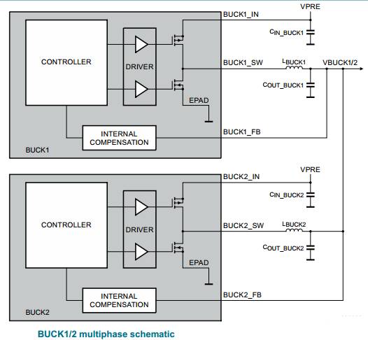
Use the OTP_VB12MULTIPH bit to enable bi-phase mode. In order to obtain the best EMC performance, the PCB layout of BUCK1 and BUCK2 must be symmetrical.
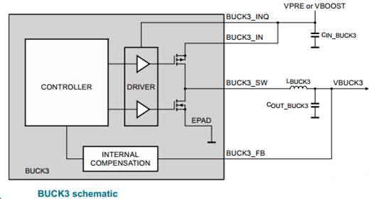
4. BUCK3
BUCK3 is a low voltage, synchronous, valley current mode BUCK converter that integrates HS PMOS and LS NMOS. BUCK1 & 2 work in PWM mode, and the output voltage can be set from 1.0V to 3.3V through OTP. Its operating frequency is 2.22MHz, and the output current is limited to 3.6A peak. The input source of BUCK3 can be connected to the output terminal of VPRE or VBOOST.
The typical application block diagram is as follows:
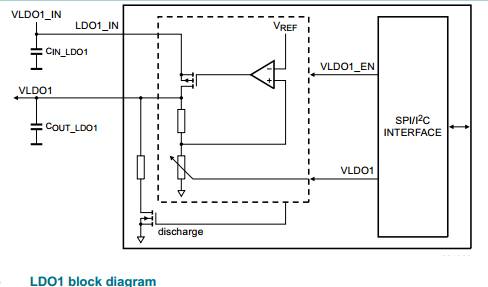
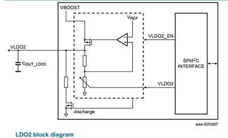
5. LDO1 & 2
LDO1 & 2 are two linear regulators. The output voltage can be set from 1.1V to 5.0V through OTP. Its current output capability is determined by its minimum voltage drop (150mA is 0.5V, 400mA is 1.0V).
The input power of LDO1 is connected externally to VPRE, VBOOST or other power sources. The LDO2 input power supply is internally connected to the output of VBOOST. The typical application block diagram is as follows:
6. I/O interface
6.1 WAKE1 & 2
The WAKE pin is used to manage the internal bias of the device and the conversion of the main state machine. The specific conversion conditions are as follows:
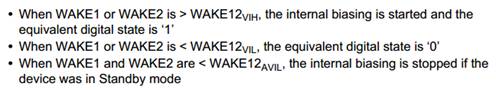
WAKE1 & 2 are level-based wake-up input signals, with the ability to perform analog measurement through AMUX. For example,
WAKE1 can be connected to VBAT, and WAKE2 can be connected to the wake-up output of CAN or FlexRay transceiver.
6.2 INTB
INTB is an open-drain output pin, which is internally pulled up to VDDIO. When an internal, this pin generates a pulse to notify the microcontroller. Set the corresponding prohibition in the M_INT_MASK register, and control each entry once.
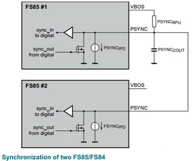
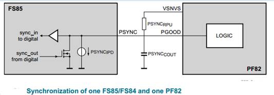
6.3 PSYNC
The PSYNC function allows multiple power management ICs to manage the input sequence, such as two FS85/FS84 (OTP_PSYNC_CFG = 0) or one FS85/FS84 plus one PF82 (OTP_PSYNC_CFG = 1).
When using PSYNC to synchronize two FS85/FS84, the PSYNC pins of each device should be connected together and pulled up to the VBOS pin of the FS85/FS84 master device. In this configuration, the FS85#1 state machine will be in the FS85 Stop before #1_VPRE and wait for FS85#2 to synchronize FS85#2_VPRE to start, as shown in the figure:
When using PSYNC to synchronize a FS85/FS84 and a PF82, the PSYNC pin of FS85/FS84 should be connected to the PGOOD pin of PF82 and can be pulled up to the VSNS pin of PF82. In this configuration, the FS85 state machine stops after VPRE starts, and waits for the release of PF82_PGOOD to continue its own power-on sequence. It allows synchronizing the respective power start sequence of two devices. During the power-off process, FS85 should wait for the completion of the PF82 power-off procedure before turning off VPRE (VPRE is supplying power to PF82). OTP_VPRE_off_dly bit should modify its configuration from the default 250μs to 32ms. as the picture shows:
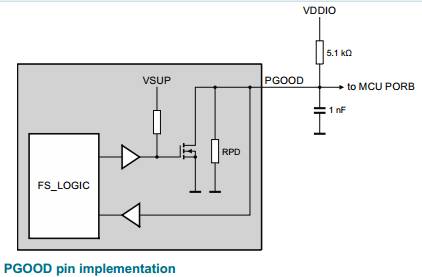
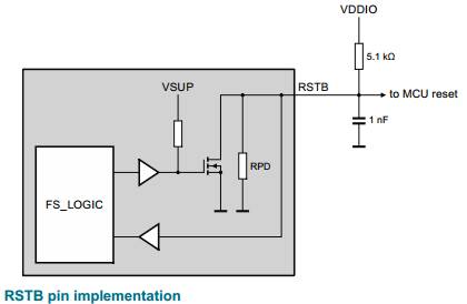
7. PGOOD & RSTB
PGOOD is an open-drain output used to connect to the PORB of the MCU. PGOOD needs an external pull-up resistor to VDDIO and a filter capacitor to GND to prevent malfunction caused by interference. Refer to the picture below:
RSTB is an open-drain output, used to connect to the RESET of the MCU. RESTB requires an external pull-up resistor to VDDIO and a filter capacitor to GND to prevent malfunction caused by interference. Refer to the picture below:
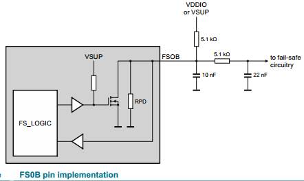
8. FS0B
FS0B is an open-drain output used to send a safe state to the system. FS0B needs an external pull-up resistor to VDDIO or VSUP. FS0B needs a 10nF filter capacitor to GND or an RC filter network when used in local or entire global systems to prevent interference from causing malfunctions. Refer to the picture below:
Three, LAYOUT guide
1. Device selection
SMPS input and output capacitors should be low ESR (ceramic or MLCC type capacitors). X7R ceramic type is best. The input decoupling capacitor should be as close as possible to the device pins. The rated voltage of the output capacitor should be selected as 3 times the voltage output value to minimize the degradation of the DC deviation.
SMPS inductors should be shielded inductors with an ISAT value higher than the maximum Inductor peak current.
2. VPRE
The design of the inductor charging and discharging current loop should be as close as possible.
The input decoupling capacitor should be placed close to the drain pin of the high-side transistor.
The boot strap capacitor should be placed close to the pin of the device and connected to the drain pin of the external low-side transistor using a wide and short trace.
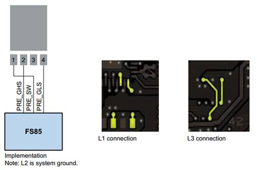
The PRE_GLS, PRE_GHS and PRE_SW traces should be wide and short, and should not cross any sensitive signals (such as current detection signals). as the picture shows:
PRE_FB, as a voltage feedback and current detection signal, should be connected to the VPRE output capacitor and paired with CSP to reduce interference and improve output accuracy.
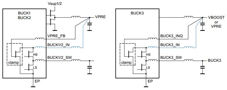
3. VBUCKx
The design of the inductor charging and discharging current loop should be as close as possible. as the picture shows:
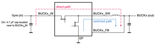
The input decoupling capacitor should be placed close to the BUCKx_IN pin.
The BUCK3_FB and BUCK3_INQ pins should be connected to the same capacitor. The input source of BUCK3_IN determines the selection of the VPRE or VBOOST output capacitor (in the blue path below, the coil inductance is parasitic to the wiring. In Japan , The coil is parasitic to bonding.) As shown in the figure:
The Links: CM300DXD-24A DMF682AN-EW


