

“Gallium Nitride (GaN) is the closest device to an ideal semiconductor switch, enabling power conversion with very high energy efficiency and high power density. But GaN devices are in some ways less robust than older silicon technologies, so they need to be used with care, and integrating the right gate drive is critical for optimal performance and reliability. This article looks at these issues and presents a driver solution that addresses the risks of the design process.
“
Gallium Nitride (GaN) is the closest device to an ideal semiconductor switch, enabling power conversion with very high energy efficiency and high power density. But GaN devices are in some ways less robust than older silicon technologies, so they need to be used with care, and integrating the right gate drive is critical for optimal performance and reliability. This article looks at these issues and presents a driver solution that addresses the risks of the design process.
text
Gallium Nitride (GaN) HEMTs are the poster child for power converters with end-to-end energy efficiency higher than today’s silicon-based solutions, easily exceeding the strictest 80+ specifications for servers and cloud data centers or the EU Code of Conduct Tier for USB PD external adapters 2 standard. While older silicon-based switching technology claims near-ideal performance for fast, low-loss switching, GaN devices are closer but not directly replaceable. To fully exploit the potential benefits of this technology, external driver circuits must be matched to the GaN device and carefully laid out.
Comparing GaN and Silicon Switches
Higher energy efficiency is the main potential advantage of enhancement-mode GaN over silicon (Si) switches. Unlike depletion-mode GaN, enhancement-mode GaN is typically an off device, so it requires a positive gate drive voltage to turn on. The higher energy efficiency of enhancement-mode GaN stems from the lower device capacitance and the reverse (third quadrant) conductivity of GaN, but zero reverse recovery charge, a major advantage for hard-switching applications. Low gate-source and gate-drain capacitance, resulting in low total gate charge, enabling gate driver fast gate switching and low losses. Additionally, low output capacitance provides lower turn-off losses. Other differences that may affect actual GaN performance are the lack of drain-source/gate avalanche voltage ratings and the relatively low absolute maximum gate voltage, about +/-20V for Si MOSFETs, while GaN is typically only +/-10V. In addition, the turn-on threshold (VGTH) of GaN is about 1.5V, which is much lower than that of Si MOSFET (about 3.5V). If external drive and load circuits can reliably control source and gate voltages, switching frequencies can reach into the hundreds of kHz or MHz region, maintaining high energy efficiency, reducing magnetics and capacitor size, and providing high power density.
GaN gate drive critical to performance
Keeping the gate drive voltage within the absolute maximum limit is not the only requirement. For the fastest switching, a typical GaN device needs to be driven to an optimal VG(ON) value of about 5.2V for full enhancement without requiring additional gate drive power. The driving power PD is obtained by the following formula:
where VSW is the total gate voltage swing, f is the switching frequency, and QGTOT is the total gate charge. Although the GaN gate has effective capacitive characteristics, power is dissipated in the effective series resistance of the gate and in the driver. Therefore, it is important to keep the voltage swing to a minimum, especially at very high frequencies. Typically, for GaN, QGTOT is a few nC, about one-tenth the value of a similar silicon MOSFET—one of the reasons GaN can switch so fast. GaN devices are charge controlled, so for nanosecond switching with nanoCoulomb gate charge, the peak current is the amplifier stage and must be supplied by the driver while maintaining a precise voltage.
In theory, GaN devices turn off safely at VGS = 0, but in the real world, the voltage applied directly to the gate is unlikely to be 0V for even the best gate drivers. According to VOPP = -L di/dt (Figure 1), any series inductance L in the source lead common to the gate drive loop will produce an opposite voltage VOPP to the gate drive, which will result in false switching of high source di/dt. The same effect can be caused by the off-state dv/dt forcing current through the device’s “Miller” capacitance, but for GaN this is negligible. One solution is to provide a negative gate turn-off voltage, maybe -2 or -3V, but this complicates the gate drive circuit, which can be avoided by careful layout and use of ‘Kelvin connections’ and with the smallest package Inductive devices such as low-profile, lead-free PQFN packages.
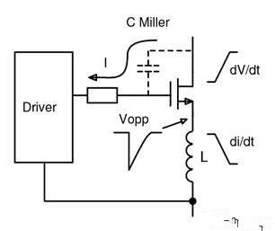
Figure 1: Inductance common to source and gate drives causes voltage transients
Challenges of high-side gate drive
GaN devices are not necessarily suitable for all topologies, as most “single-ended” flybacks and forwards do not have reverse conduction, and their additional cost over silicon MOSFETs outweighs any small efficiency benefits. However, “half-bridge” topologies – totem-pole bridgeless PFCs, LLC converters, and active-clamp flybacks – will naturally be a stronghold for GaN, both hard and soft switching. These topologies have “high-side” switches whose source is a switch node, so the gate drive is canceled by a high-voltage and high-frequency waveform with nanosecond levels. The gate drive signal is referenced to the system ground by the controller, so the high-side driver must combine level shifting with an appropriate withstand voltage rating (usually 450 V or higher). It also requires a way to generate low-voltage power rails for high-side drive, typically using a network of bootstrap diodes and capacitors, referenced to the switch node. The switching waveform stress is dV/dt, and GaN can reach more than 100 V/ns. This causes displacement current to flow through the driver to ground, potentially causing transient voltages across the series resistance and connecting inductance that can damage the sensitive differential gate drive voltage. Therefore, the driver should have strong dV/dt immunity.
To minimize catastrophic “shoot-through” and achieve optimal energy efficiency, the half-bridge high-side and low-side devices should be driven without overlap while maintaining minimal dead time. Therefore, the high-side and low-side drivers should have very well-controlled, matched propagation delays.
For the low side, the ground driver should be Kelvin connected directly at the switching source to avoid common mode inductance. This can be a problem as the drive also has a ground signal which might not be the best connection. Therefore, the low-side driver may employ isolation or some method of separating power and signal, with some degree of common-mode voltage tolerance.
GaN drivers may require safety isolation
Enhancement-mode GaN devices are now receiving significant attention for off-line applications that require a high voltage rating of at least 600 V for the device and its driver, but lower voltage applications are becoming more common. If the drive input signal is generated by the controller and the connection is manually accessible through the communication interface, the drive will require safety isolation according to the relevant code. This can be achieved with appropriate isolation voltages by means of high-speed signal galvanic isolators. Maintaining the driver signal edge rate and high-low-side matching becomes an issue for these layouts, and although controller circuits are often allowed to be ‘primary-referenced’, this is the norm in most AC-DC converters anyway.
Application Example C ‘Active Clamp Flyback’
This is an example of an active-clamp flyback topology (Figure 2) that uses a high-side switch to recycle the leakage inductance energy of the converter transformer. Compared to “buffered” or hard zener clamp methods, higher energy efficiency, better EMI, cleaner leakage waves, and lower power consumption for circuit applications, between 45W and 150W, typical applications include USB PD enabled cell phones and Travel adapter for laptops, and built-in power supply.
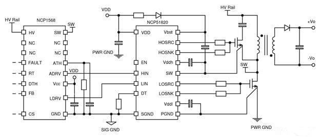
Figure 2: Overview of GaN Active Clamp Flyback Converters
Figure 2 shows ON Semiconductor’s dedicated GaN gate driver for the NCP51820[1]and NCP1568[2]Active clamp flyback controller (details omitted). The driver employs gate drivers with regulated +5.2V amplitude for high-side and low-side optimum enhancement mode GaN. Its high-side common-mode voltage range is -3.5V to +650V, low-side common-mode voltage range is -3.5 to +3.5V, dv/dt immunity is 200 V/ns, and advanced junction isolation technology is used. If there is a current sense resistor at the source of the low-side device, the low-side drive level shifting makes the Kelvin connection easier. The rise and fall times of the drive waveform are 1ns, the maximum propagation delay is 50ns, and the high and low sides provide independent source and sink outputs to customize the gate drive edges for the best EMI/efficiency trade-off. In this topology, the high- and low-side drivers do not overlap, but have different pulse widths to enable power conversion/regulation with drain clamping and zero-voltage switching controlled by the NCP1568 device.
Application Example C LLC Converter
At power levels greater than 150 W, resonant LLC converters are often used due to their high energy efficiency and limited switching voltage stress. A feature of this converter is that the drive waveform is 50% duty cycle, regulated by frequency conversion. Therefore, it is important to control the dead time to ensure that no overlap occurs. Figure 3 shows the typical architecture of the NCP13992 high-performance LLC controller. This design can operate at a switching frequency of 500 kHz and is commonly used in high-power gaming adapters and embedded power supplies for OLED TVs, all-in-one PCs.
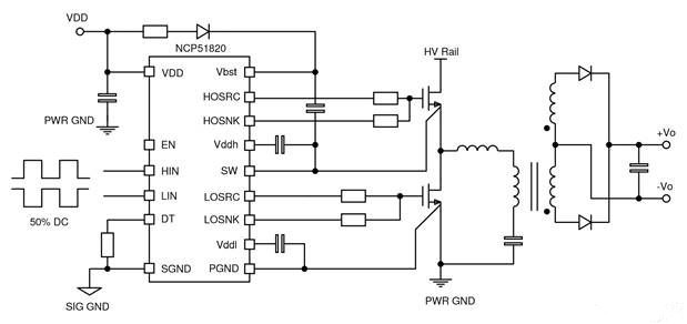
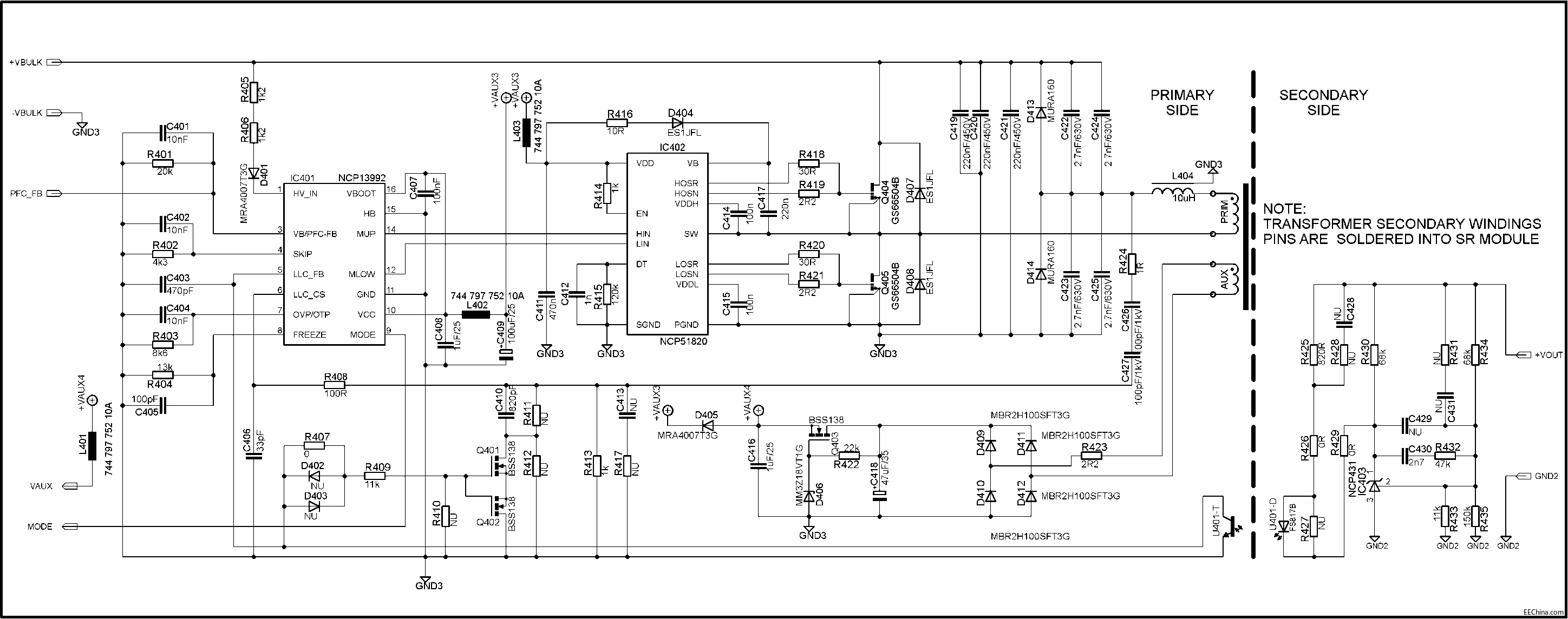
Figure 3: Overview of GaN-based LLC converters
The ON Semiconductor NCP51820 driver shown ensures that the gate drives do not overlap, but this can be disabled depending on topological needs (such as current-fed converters). The device also includes an enable input and comprehensive protection against power supply undervoltage and overtemperature. It comes in a PQFN, 4 x 4mm 15-lead package that enables short, low inductance connections to the gate of the GaN device.
Layout Considerations
In all applications, layout is the key to success. Figure 4 shows an example layout using ON Semiconductor’s NCP51820, miniaturized and matched to the gate drive loop. GaN devices and drivers are placed on the same side of the PCB, avoiding high current vias by using ground/return planes appropriately.
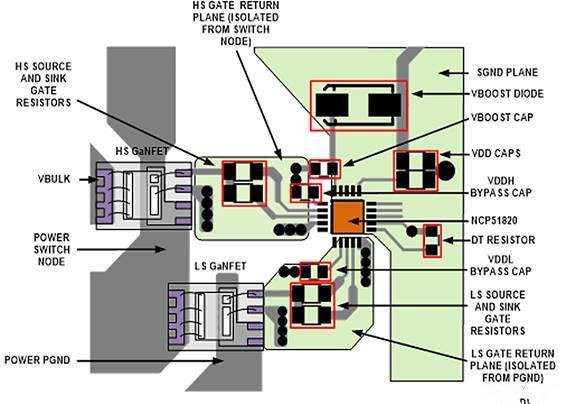
Figure 4: Good layout for a GaN gate driver circuit
Summarize
For GaN switches, the gate drive circuits need to be carefully designed to achieve higher energy efficiency, power density, and reliability in practical applications. In addition, careful layout, the use of dedicated drivers such as ON Semiconductor’s NCP51820, and a range of features for high- and low-side drivers ensure that GaN devices operate at optimum performance.
The Links: ER057003NCU G121S1-L02 LCD-DISPLAY

