
Design of Communication Countermeasure Teaching Demonstration System Based on EPlKl00 Chip and AD9854 Frequency Synthesizer
“What FPGA chip adopts is EPlKl00 chip of ACEXlK series products of Altera Company. It is characterized by the combination of look-up table (LUT) and EAB, which provides an efficient and inexpensive structure. LUT-based logic provides optimized performance and efficiency for datapath management, register strength, mathematical computation or digital signal processing (DSP) designs, while EAB can implement RAM, ROM, dual-port RAM or FIFO functionality.
“
Authors: Luo Yong, Du Jun
1 Overview
Spread spectrum communication has the advantages of strong anti-interference ability and good concealment. It has become the most important technical means in communication confrontation and anti-anti-counterfeiting. It has been paid more and more attention in military communication. Frequency hopping radio is an important part of spread spectrum communication in the military field. application. How to effectively counter the frequency hopping radio in the communication countermeasure is a hot issue at present. In the teaching of communication confrontation, in order to show people the principle of interference and anti-jamming in frequency hopping communication in the form of experiments, and to conduct reconnaissance of frequency hopping communication and compare the effects of implementing various interferences, it is helpful for scientific research to find out the principle of frequency hopping communication. The most effective interference mode of communication provides effective data and reference. This paper presents the design and implementation of a hardware solution in a communication confrontation teaching demonstration system based on DDS and USB technology.
2 System overall structure design and principle description
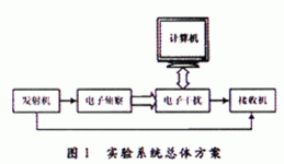
The system is mainly composed of five parts: control computer, transmitter, Electronic reconnaissance module, electronic jamming module and receiver, as shown in Figure 1. The computer is mainly used to control and coordinate the work and data transmission of each module, determine the work mode of each part of the system and monitor the work status in real time.
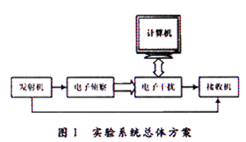
Under the control of computer instructions, the transmitter transmits frequency hopping signals in a corresponding manner within the designated working frequency band. The electronic reconnaissance module uses high-speed A/D sampling technology and high-speed FFT real-time processing technology to quickly capture and calculate the operating frequency point of the transmitted signal, and at the same time send the detected frequency hopping data to the electronic interference module. The jamming module that receives the reconnaissance data uses FPGA to control the frequency synthesis device to generate various modulation signals under the control of the computer, and selects different jamming methods to effectively jam the communication station in real time. The interference signal and the actual frequency hopping signal are respectively sent to the combiner, and the combiner is sent to the receiver to compare the actual effects of various interference methods.
3 Device selection
3.1 A/D chip and FPGA chip
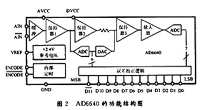
The A/D chip selected is AD6640, a 12-bit IF fast sampling chip introduced for broadband and multi-channel digital wireless receiver systems.
The AD6640 is a high-speed, high-performance, low-power, monolithic 12-bit AD converter that includes a sample-and-hold circuit and a reference source. It is powered by a single power supply +5 V, TTL/CMOS compatible level output, the typical value of IF sampling frequency is 70 MHz (multi-channel) and 200 MHz (single-channel), the sampling rate can reach 65 Mb/s, the signal The typical SNR value is 68 dB, the SFDR value is 80 dB, and the power consumption is 710 mW. AD6640 adopts the conversion structure of two-stage sub-area, which not only ensures the accuracy but also reduces the power consumption. Its functional modules are shown in Figure 2. It can be seen from Figure 2 that all the required functions of the ADC, including input buffering, track-and-hold amplification, digital error correction, and a 2.4 V reference voltage, are provided by the chip, making its design easier.
What FPGA chip adopts is EPlKl00 chip of ACEXlK series products of Altera Company. It is characterized by the combination of look-up table (LUT) and EAB, which provides an efficient and inexpensive structure. LUT-based logic provides optimized performance and efficiency for datapath management, register strength, mathematical computation or digital signal processing (DSP) designs, while EAB can implement RAM, ROM, dual-port RAM or FIFO functionality. This makes ADEXlK suitable for complex logic and memory functions, such as digital signal processing, wide-area data path management, data conversion, and various high-performance communications applications such as microprocessors. Based on reconfigurable CMOS SRAM cells, the ACEX1K architecture has all the features needed to implement common gate array megafunctions, and the corresponding high pin count provides an efficient interface to system components. Advanced processing capabilities and low voltage requirements of 2.5 V make the AC2EX1K device suitable for inexpensive, high-capacity applications.
3.2 DDS chip
The DDS chip selected is the DDS device AD9854 produced by the American Analog Device Inc (ADI) company. The AD9854 digital frequency synthesizer is a highly integrated device using advanced DDS technology.
He has a pair of internal high-speed, high-performance quadrature D/A converters and comparators, which can realize digital synthesis of quadrature I and Q outputs. When an accurate reference frequency is input, the AD9854 can generate a highly stable frequency, phase, and amplitude programmable sine and cosine signals. The DDS core of the AD9854 has a frequency resolution of 48 b. The 14 b phase truncation guarantees excellent SFDR performance. The circuit technology of the AD9854 enables the synchronous quadrature signal output frequency up to 150 MHz, generating an average of 1 million new frequencies per second. The programmable reference frequency accumulator of 4 to 20 integer multiples in AD9854 can convert the low-speed clock input from the outside into an internal high-speed clock (up to 300 MHz).
The AD9854 can implement Ramped FSK with enhanced spectral characteristics in addition to the basic FSK. The device uses advanced 35μmC2MOS technology so that the device only needs +3.3 V power supply.
3.3 DAC chip and USB chip
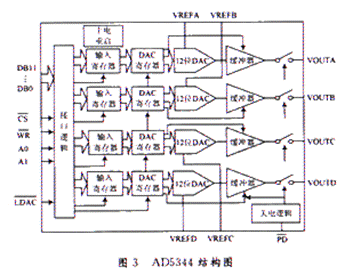
The DAC used in the system is AD5344 of Analog Devices, which is a low-power 12 b digital-to-analog converter. The chip can be used in portable battery power instruments, programmable voltage and current sources, programmable attenuators, industrial processing controllers, and digital amplification and compensation regulation. Figure 3 is a schematic diagram of its internal structure. AD5344 has four 12 b DACs, which can work normally between 2.5 and 5.5 V, and the typical current value is 500 μA when the external +3 V voltage is connected, and it has a power saving mode that further reduces the current to 80 nA. Its output buffer drives the output over two power rails. Which output channel is selected can be controlled through A0 and A1.
The LISB chip in the control module is FT245BM from FTDI Company. This chip is a general-purpose special-purpose chip that supports the USB 1.1 standard produced by FTDI in the early days. Programming use, greatly shorten the development cycle.
The block diagram of the internal structure of FT245BM is shown in Figure 4. The internal structure of FT245BM is mainly composed of USB transceiver, serial interface engine (SIE), USB protocol engine and first-in-first-out (FIFO) controller. One of its obvious advantages is that the internally integrated modules are fully functional and do not need to be reconfigured during use. After receiving the control command sent by the host, the USB transceiver automatically executes the command, and completes the serial/parallel bidirectional conversion of USB data through the serial interface engine. The USB protocol engine completes the management of the FIFO controller according to the USB 1.1 specification. The FIFO controller guides the external host controller to read and write control to the USB chip through its two handshake signal output ports RXF# and TXE#.
4 Design and implementation of the system
4.1 Design of Interference Module
The schematic diagram of the interference module is shown in Figure 5. In the design of the interference module, the commonly used DDS chip AD9854 combined with FPGA is selected to generate the interference frequency. In order to realize the controllability of the power of the interference signal, an attenuator is planned to be added to the signal output by the DDS. A computer is used to control the selection of the interference mode and the selection of the parameters of the interference signal through the USB chip. The signal generated by DDS is first low-pass filtered and then amplified to suppress spurious signals.
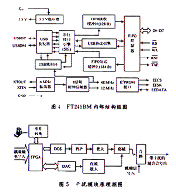
In the tracking jamming, the FPGA receives the communication signal obtained by the electronic reconnaissance, and guides the DDS to generate the jamming signal of the same frequency. In the non-tracking interference, the interference signals of single frequency interference, frequency sweep interference and random frequency modulation noise are generated by computer control. These interference signals and the original frequency hopping signal are combined and output in the combiner and sent to the frequency hopping receiver. , in order to test the anti-interference ability of frequency hopping communication to these interference patterns.
4.2 Design of the control module
In the overall design process of the system, a very important part is the control of the entire experimental system. The block diagram of the overall control module of the system is shown in Figure 6.
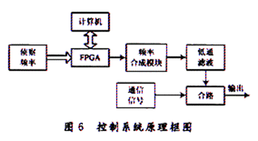
As can be seen from the figure, the FPGA chip in the interference module plays a central role in system control. In this module, FPGA mainly completes four tasks:
(1) Realize real-time communication with the electronic reconnaissance module, continuously receive the frequency hopping signal information sent by the reconnaissance module, and make corresponding responses immediately.
(2) Realize the communication with the computer host, control the read and write programs of the USB chip, receive the control commands sent by the host at any time, and complete the corresponding functions.
(3) Realize the control of the DDS chip, and select different working modes of the DDS according to the needs.
(4) Realize the control of the attenuator, and select different frequency amplitudes according to the command of the host.
5 Conclusion
Through the analysis and debugging of the actual hardware circuit, the system realizes the control of the USB chip by the computer, the control of the DDS chip by the FPGA, the interconnection and communication between the reconnaissance module and the interference module, and the controllable realization of various interference methods. In the actual test, by comparing the effects of different jamming methods, the most effective jamming mode for frequency hopping radio communication can also be selected, and it has certain practical reference significance for future research on the actual combat form of frequency hopping reconnaissance jamming system.
The Links: B104SN01-V2 LM170E03-TLG6

