
Zero-Drift Precision Op Amp: Measure and Eliminate Aliasing for More Accurate Current Sensing
“Zero-drift precision op amps are specialized op amps designed for applications that require high output accuracy due to small differential voltages. Not only do they feature low input offset voltage, they also feature high common-mode rejection ratio (CMRR), high power-supply rejection ratio (PSRR), high open-loop gain, and low drift over a wide temperature and time range (see Table 1). These features make it ideal for applications such as low-side current sensing and sensor interfacing, especially with very small differential signals.
“
Zero-drift precision op amps are specialized op amps designed for applications that require high output accuracy due to small differential voltages. Not only do they feature low input offset voltage, they also feature high common-mode rejection ratio (CMRR), high power-supply rejection ratio (PSRR), high open-loop gain, and low drift over a wide temperature and time range (see Table 1). These features make it ideal for applications such as low-side current sensing and sensor interfacing, especially with very small differential signals.
Table 1. Key parameters affecting op amp accuracy and precision.
|
key parameter |
symbol |
unit |
importance |
|
Input offset voltage |
VOS or VIO |
µV |
The lower offset enables accurate measurement of lower differential voltages. |
|
Input offset voltage drift |
dVOS/dT or ΔVOS/ΔT |
µV/°C |
The lower drift prevents the offset voltage from changing with temperature. |
|
Common Mode Rejection Ratio |
CMRR |
dB |
A high CMRR indicates that the offset voltage is less susceptible to common-mode voltage variations. |
|
Open loop voltage gain |
AVOL |
dB |
High open-loop gain results in better closed-loop gain accuracy. |
|
power supply rejection ratio |
PSRR |
dB |
High PSRR means that the offset voltage is less susceptible to power supply variations. |
While zero-drift op amp manufacturers sometimes claim that these devices have no aliasing effects, in reality they can be prone to aliasing because these devices use sampling to minimize input offset voltage. Therefore, designers should test their op amp circuits for aliasing effects.
Traditional methods of detecting aliasing using a spectrum or network analyzer have proven insufficient, so designers are advised to use a measurement technique that sweeps the input across a frequency range and observes the op amp output on an oscilloscope. This article applies this test method to different op amps to see how different zero-drift op amps differ in aliasing. Devices tested included auto-zero and chopper-stabilized types from ON semiconductor and competitors.
This article first describes the impact of input offset voltage on op amp performance, and the performance differences between zero-drift, chopper-stabilized op amps and general-purpose op amps. Next, we describe the operation of chopper-stabilized op amps and how the sampling that occurs in these amplifiers causes aliasing when the input signal approaches or exceeds the op amp’s offset correction frequency. The chopper-stabilized architecture is not the only way to implement a zero-drift op amp, and the chopper-stabilized architecture was compared to another zero-drift architecture called auto-zeroing.
After giving aliasing measurements for various op amps, this article explains how Nyquist sampling theory determines the allowable input frequency range without aliasing, and how to apply a simple low-pass filter to prevent aliasing stack. Subsequent sections of this article illustrate the relationship between op amp input offset voltage and other parameters such as transient response, start-up time, rail-to-rail operation, low-frequency noise, and input current in zero-drift op amps. Finally, it is explained that the SPICE model cannot account for zero-drift effects like aliasing.
Why is input offset voltage important?
Offset voltage is one of the parameters that limits the smallest signal that can be captured reliably. This defines a low dynamic range level.
Input offset voltage is a critical parameter for all op amps. In datasheets it is often referred to as VOSor VIO. It is the inherent differential voltage between the IN+ and IN- terminals and measures how well the input pair is matched. For an ideal op amp, in a closed loop system VIN+ = VIN-. In the real world, due to the input offset voltage, VIN-will not be equal to VIN+.
Although there are some silicon-level design techniques that can be used to improve input pair matching, the manufacturing process is a major contributor to the input offset voltage. Defects in semiconductor materials cause internal voltage differences between input pins. Different types of defects caused by the manufacturing process produce different temperature coefficients.
This device-to-device variation can cause device-specific drift (input offset voltage drift over temperature) to be higher or lower than the typical value on the data sheet. In addition, the drift coefficient variation with temperature may be positive or negative. This makes it difficult to simply calibrate the input offset voltage in the application. In some cases, reducing the offset or drift in conventional linear op amps results in a loss of power consumption.
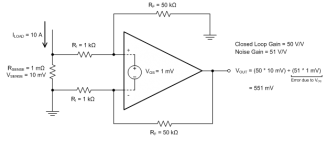
The input offset voltage is multiplied by the gain and added to the output voltage, essentially adding an error factor to the output, as shown in Figure 1. This parameter becomes critical when measuring small differential voltages. As the differential voltage decreases, the error due to the input offset voltage increases.

Closed Loop Gain: closed loop gain
Noise Gain: noise gain
Error due to Vcc: Error due to Vcc
Figure 1. Current sensing with an op amp in a differential amplifier configuration. Low offset voltage is critical because input offset voltage is amplified by noise gain, creating offset errors at the output.
In the differential amplifier circuit shown in Figure 1, the output voltage is the sum of the signal gain term and the noise gain term:
As an internal op amp parameter, the input offset voltage is multiplied by the noise gain instead of the signal gain. This will result in output offset errors.
A precision amplifier that minimizes this offset, using a variety of techniques to reduce the input offset voltage. For zero-drift amplifiers, this is especially true for low frequency and DC signals. Table 2 compares the maximum input offset of commonly used general-purpose op amps with chopper-stabilized zero-drift amplifiers.
Table 2. Comparing the maximum offset voltage of common general-purpose op amps and chopper-stabilized zero-drift op amps.
|
device |
instruction |
Maximum VOS @ 25°C |
|
LM321[1] |
Traditional General Purpose Operational Amplifier |
7000µV |
|
NCS20071[2] |
General purpose operational amplifier |
3500µV |
|
NCS21911[3] |
Chopper Stabilized Zero Drift Operational Amplifier |
25µV |
|
NCS333A[4] |
Chopper Stabilized Zero Drift Operational Amplifier |
10µV |
What is a zero-drift operational amplifier?
Precision op amps can achieve “zero-drift” offset voltage, maintaining low input offset voltage over temperature and time through a variety of techniques. One of the ways amplifiers can accomplish this is by using a design technique that periodically measures the input offset voltage and corrects the offset at the output. This structure is called a chopper-stabilized structure.
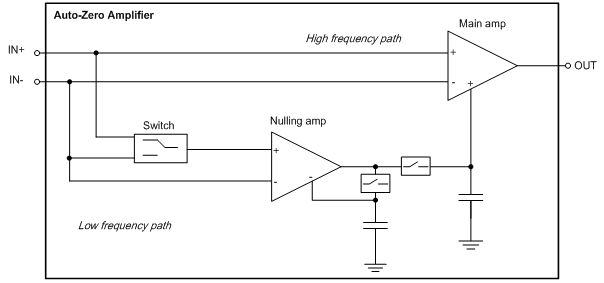
Like all engineering solutions, zero-drift op amps have their limitations. A less obvious reason is that the internal circuitry of a chopper-stabilized amplifier contains a clocking system. ON Semiconductor’s NCS333[4]and NCS21911[3] A simplified block diagram of the chopper-stabilized structure used in Figure 2.
While some might argue that this type of chopping is a real-time system, practice has shown that it is susceptible to aliasing or heterodyne problems with classical sampling systems. The main artifact of chopper-stabilized op amps occurs when the signal approaches the clock frequency of the chopper. This article uses the term aliasing, but the problem involved might be more appropriately called heterodyne.
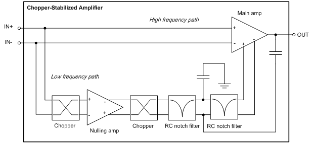
Chopper-Stabilized Amplifier: Chopper-Stabilized Amplifier
High frequency path: High frequency path
Main amp: main amplifier
Low frequency path: low frequency path
Chopper: Chopping
Nulling amp: Nulling Amplifier
RC notch filter: RC notch filter
Figure 2. Simplified block diagram of a chopper-stabilized op amp
In Figure 2, the lower signal path is where the chopper samples the input offset voltage, which is then used to correct the output offset. This offset correction frequency is within the overall bandwidth of the amplifier. Because this structure uses sampling, best performance occurs when the input signal frequency is kept below the relevant Nyquist frequency.
This means that the input signal frequency not only needs to be within the closed-loop bandwidth, but also within half of the offset correction frequency for optimum performance. This allows the chopper to maintain a sampling frequency higher than the Nyquist rate, eliminating the possibility of aliasing. When the signal frequency exceeds the Nyquist frequency, aliasing may occur at the output. This is an inherent limitation of all chopper and chopper-stabilized architectures due to the use of a sampling system.
The chopper-stabilized structure benefits from having a feedforward path, shown in the upper signal path of the block diagram in Figure 2, which is a high-speed signal path that extends the gain bandwidth beyond the sampling frequency. Not only does this help preserve the high frequency components of the input signal, but it also improves the loop gain at low frequencies. Assume that the open loop gain of the op amp drops by -20 dB/decade. As the unity-gain bandwidth increases, the graph also shifts toward higher gains.
An example is given in Figure 3. When the op amp is placed in a closed-loop system, the open-loop gain of the system increases, improving the closed-loop accuracy of the system. This is especially useful for low-side current sensing and sensor interface applications, where the signal is low frequency and the differential voltage is relatively small.
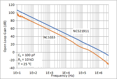
Figure 3. Open-loop gain as a function of frequency of two chopper-stabilized amplifiers. The higher bandwidth NCS21911 shows how increasing the unity-gain bandwidth also increases the overall open-loop gain. The increased open-loop gain improves the accuracy of closed-loop systems, even for DC systems.
However, not all zero-drift amplifiers are created equal. Different implementations of the architecture may have different results. Even due to sampling constraints, ON Semiconductor’s NCS333 and NCS21911 series of op amps have minimal aliasing compared to competing devices from other manufacturers and are less susceptible to aliasing effects. This is because ON Semiconductor’s patented scheme uses two cascaded, symmetrical, RC notch filters tuned to the chopping frequency and its 5th harmonic to reduce aliasing effects.
Another zero-drift architecture is called “auto-zeroing”. The block diagram of the auto-zeroing architecture shown in Figure 4 is similar to the chopper-stabilized architecture, but implemented differently. The auto-zero architecture has a main amplifier and a zero-stabilizing amplifier. This method also uses the clock system.
In the first stage, the switched capacitor maintains the offset error of the previous phase at the output of the stabilizing amplifier. In the second stage, the offset of the main amplifier is corrected by the offset of the output of the zero-stabilizing amplifier. The structural differences between auto-zeroing and chopper-stabilized amplifiers lead to differences in noise performance and aliasing sensitivity, which are discussed in later chapters.
Auto-Zero Amplifier: Auto-Zero Amplifier
High frequency path: high frequency path
Main amp: main amplifier
Switch: switch
Nulling amp: Nulling Amplifier
Low frequency path: low frequency path
Figure 4. Simplified block diagram of an auto-zero op amp
Determining the Zero-Drift Amplifier Clock Frequency
Many zero-drift amplifier data sheets do not provide information on the internal clock frequency. Occasionally, it may be mentioned in a paragraph of the application section. Sometimes the clock frequency in question can be identified by noise or perturbations in the bandwidth plot. Therefore, it is up to the user to test whether the circuit is susceptible to aliasing.
The method shared here is very simple: it involves sweeping the amplifier input to the gain bandwidth product over a range of frequencies while observing the op amp output on an oscilloscope. To the best of the authors’ knowledge, the internal clock frequencies of all known zero-drift amplifiers are within the amplifier’s gain bandwidth, typically at about one third of the gain bandwidth. These amplifiers will perform best at signal bandwidths less than half that frequency.
Find and test aliasing
The datasheets for some zero-drift amplifiers claim that they have no aliasing. It can be assumed that these manufacturers tried their best to measure any possible aliasing, but found nothing. In the development of zero-drift amplifiers at ON Semiconductor, initial measurements on competing amplifiers also demonstrated no aliasing. At the time, no spurious clocks were found in the output of competitor devices. However, further testing showed that aliasing of these devices could still be found using simple oscilloscope-based measurement techniques.
Customers have reported problems with systems using zero-drift op amps from some manufacturers and found aliasing. In these cases, the common theme is where the signal of interest, low frequency or DC signal has superimposed high amplitude, high frequency interference or ripple signals. Results for end systems vary, including closed-loop systems stabilizing under incorrect conditions and systems failing to report the correct signal.
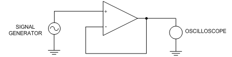
Past efforts to find aliasing have involved the use of sophisticated spectroscopy and network analysis systems that have provided indeterminate results. For a more basic approach, connect an oscilloscope to the amplifier output for direct visual observation. For input excitation, the generator is used to sweep the input frequency at the desired clock frequency (and elsewhere as needed) to see if a “beat frequency” can be produced at the output. This approach works well, arguably one of the most linear op amp configurations, considering the original work was done with a gain configuration of +1, as shown in Figure 5.
SIGNAL GENERATOR: signal generator
OSCILLOSCOPE: Oscilloscope
Figure 5. The test circuit to detect aliasing is a simple unity-gain buffer. The essence of this technique is to view the device output on an oscilloscope. Spectrum and network analyzers don’t always seem to detect signals related to the inner workings of zero-drift amplifiers.
The first op amp selected for this test was ON Semiconductor’s NCS325 auto-zero technology amplifier, rather than a chopper-stabilized amplifier like the other devices tested. Theoretically, auto-zeroing structures will exhibit more significant aliasing effects than chopper-stabilized versions, making verification testing a convenient first choice. Figure 6 depicts the aliasing of the NCS325. Measuring familiar amplifiers for the first time makes validating these tests easy because the clock frequency is known.
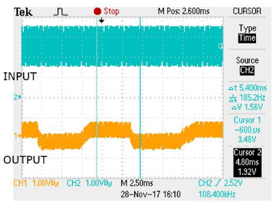
Figure 6. The aliased output of the first amplifier was tested, ON Semiconductor’s NCS325 used in a simple +1V/V buffer. The upper blue line is the input signal and the lower orange line is the aliasing seen at the amplifier output.
At this point, it’s important to remember that aliasing is not a defect of sampling amplifiers, but rather a behavior. Knowledge of this behavior, and how to avoid it, can make zero-drift amplifiers work at their best.
After checking the NCS325, the next step is to test ON Semiconductor’s chopper-stabilized amplifier NCS333. An interesting result is produced here, where the only noticeable aliasing may be found at twice the clock frequency. This suggests that performing this test to find aliasing may require sweeping across the entire bandwidth of the amplifier to detect these signals. Figure 7 depicts the aliased signal of the NCS333.
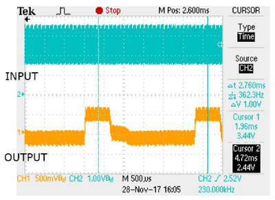
Figure 7. Aliasing of the NCS333 chopper-stabilized zero-drift op amp. This aliasing phenomenon is expected to occur near the clock frequency, but we did not find aliasing. But aliasing does appear in the second harmonic of the clock frequency.
We also performed aliasing tests on competitor zero-drift chopper-stabilized amplifiers. The popular amplifier datasheet says it has no aliasing. However, Figure 8 depicts aliasing at the fundamental frequency of the internal clock. For this amplifier, previous extensive testing with spectrum and network analyzers failed to find any indication of the clock or its frequency.
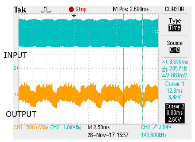
Figure 8. Aliasing of a competitor’s chopper-stabilized zero-drift op amp. The datasheet for this 5V, 350 kHz bandwidth op amp claims no aliasing.
Likewise, the NCS21911 precision op amp with a bandwidth of 2 MHz shows aliasing when the input signal is 500 kHz and the gain is about G=-1V/V, as shown in Figure 9.
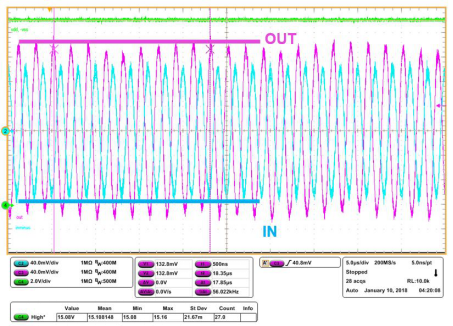
Figure 9. Aliasing of the 36V, 2 MHz precision amplifier NCS21911. Aliasing is still controlled at 500 kHz. The blue line in the center is the input signal, and the larger magenta line is the amplifier output, showing aliasing.
But under the same conditions, the aliasing of the NCS21911 is well controlled compared to its counterparts from other manufacturers, as shown in Figure 10.
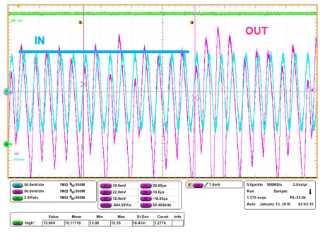
Figure 10. The aliased output of a competitor’s 36 V, 2 MHz precision amplifier exhibits more unstable behavior at the same 500 kHz signal frequency. The blue line in the center is the input signal, and the larger magenta line is the amplifier output, showing aliasing.
Another example is shown in a comparison of the NCS21911 and a competitor’s 2MHz chopper-stabilized precision op amp. The NCS21911 shows minimal aliasing in the 1MHz to 2MHz range in a unity-gain buffer circuit, as shown in Figure 11. In contrast, the competitor’s device performed normally at 1 MHz, exhibited aliasing at 1.5 MHz, and reduced aliasing at 2 MHz (along with bandwidth), as shown in Figure 12.
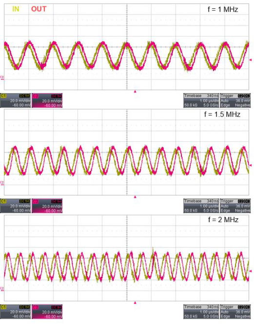
Figure 11. NCS21911 has small signal at 1 MHz (top), 1.5 MHz (middle), and 2 MHz (bottom) in unity gain circuit. Aliasing is minimal.
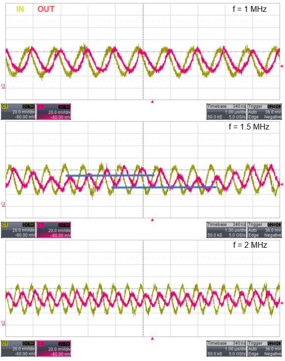
Figure 12. Competitor’s 2 MHz chopper-stabilized precision op amp has small signals at 1 MHz (top), 1.5 MHz (middle), and 2 MHz (bottom). Aliasing (marked in blue) is evident at 1.5 MHz and decreases as the input signal increases to 2 MHz. Note also the lower bandwidth of the competitor’s device, as shown in the bottom waveform.
Not every chopper-stabilized amplifier is the same. It is therefore critical to test each device over the entire operating frequency range.
Alias-prone system
When the signal of interest is accompanied by high frequency coupling of spurious signals or large high frequency ripple, the system is prone to aliasing. The results may simply consist of delivering incorrect or noisy values, or the control loop falling on an incorrect operating point.
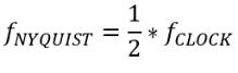
According to the Nyquist sampling theorem, the zero-drift clock should be at least twice the maximum frequency component of the signal of interest. In other words, the maximum frequency of the input signal should be less than or equal to half of the amplifier’s internal clock.
How to obey Nyquist sampling theory? Determine the upper limit of the signal frequency (fin CLOCK/2) is easy, but the pickup of spurious signals, noise or ripple may contain frequencies higher than the Nyquist frequency. These frequencies can then be mixed into the proper frequency range, resulting in false or incorrect readings.
To ensure that the frequency content of the input signal is limited to the usable frequency range, a low-pass filter can be added before the amplifier. This filter acts as an anti-aliasing filter. Reduce or eliminate aliasing effects by attenuating higher frequencies (beyond the Nyquist frequency).
The antialiasing filtering must be purely analog filtering before the amplifier input. Usually a simple RC filter is sufficient, as shown in Figure 13. No complicated filter architecture is required. Do not configure the amplifier as part of the filter in an active filter circuit.
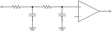
Figure 13. An anti-aliasing filter can be as simple as a two-stage RC filter. The filter must be placed in front of the amplifier input.
Cascading zero-drift amplifiers can also pose risks, as multiple clock frequencies can interact and cause aliasing.
Transient Response Considerations
Due to the time-based sampling of the chopper channel structure, the zero-drift amplifier achieves a low offset with a certain time characteristic, which means that offset correction does not occur immediately. Large dynamic steps at the amplifier input, or worse, input overload can create conditions where the loop will take time to recreate the low offset. This essentially affects stable timing and behavior.
Relatively fast recovery and settling times have been achieved using higher clock frequencies; however, these parameters are typically tens of microseconds or higher for zero-drift amplifiers. Typically, this is due to design tradeoffs. In transistor-level amplifier designs, choosing a faster settling time results in a higher offset voltage. Generally, lower input offset voltage specifications have higher priority.
On-time and robust design
Since zero-drift amplifiers contain quite a bit of logic, it is not surprising that they also include some means of ensuring specific behavior during startup and power failures such as power outages. When an offset correction amplifier is first activated, the output will reflect the uncorrected offset for a short time. Once the supply voltage reaches the trip point set by the power-on-reset (POR) circuit, the offset correction mechanism requires several clock cycles until the output of the amplifier reaches the specified offset voltage limit.
Typically, amplifier startup time is not a critical item from a system-wide perspective, as it is usually within the startup time of the overall system. This is probably why many op amp manufacturers do not show this parameter in their zero-drift amplifier datasheets. It should be noted that the start-up time also depends on the configuration gain of the amplifier – a larger gain increases the overall start-up time.
In very critical systems, consideration should be given to the fact that linear amplifiers simply eliminate these disturbances, providing more robust start-up performance. Some precision op amps use TRIM instead of chopper-stabilized or auto-zero structures to achieve low offset voltage. This use of amplifiers eliminates any clocking system. This is a key consideration in many designs such as large industrial circuit breakers. The tradeoff is that these trimmed linear amplifiers do not necessarily achieve the same ultra-low input offset voltage performance of zero-drift amplifiers.
Zero-drift effect for improved rail-to-rail performance
Rail-to-rail input op amps use two input pairs to achieve a widened common-mode input voltage range. PMOS pairs can be used as input stages for lower input voltage regions, while NMOS pairs can be used for higher input voltage regions. Each input pair has its own corresponding input offset voltage. When the common mode voltage moves from one region to another, there is usually a crossover region where the offset voltage jumps from one region to the next.
Rail-to-rail input performance in zero-drift op amps brings clear benefits compared to non-zero-drift amplifiers, significantly reducing the impact of input-stage crossover regions between PMOS and NMOS input pairs. Offset voltage and offset voltage drift performance close to the common-mode input voltage limit is excellent, so zero-drift amplifiers are also commonly used in applications such as high-side current sensing.
Effect of zero drift on low frequency noise
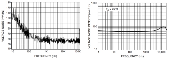
Zero-drift chopper-stabilized amplifiers are ideal for precise, high-gain amplification at lower frequencies. Typically, they do not exhibit the higher bandwidth of linear op amps, and the location of their clock frequency establishes a practical frequency limit for signal fidelity, as described in the section on aliasing. This makes performance at low frequencies particularly important, and the chopper-stabilized architecture further contributes to low frequency availability by eliminating the classic linear op amp 1/f input voltage noise (see Figure 14).
Many high-gain sensor applications are at low frequencies, making zero-drift amplifiers a natural choice for this function. Although the term “low frequency” is used here, these amplifiers typically provide excellent performance up to 100 kHz.
(a) (b)
FREQUENCY: Frequency
VOLTAGE NOISE: Voltage Noise
Figure 14. Voltage noise density plots for a conventional amplifier (NCS2005, figure (s) and a zero-drift amplifier (NCS333, figure (b)) showing the cancellation of 1/f noise in a zero-drift amplifier. Note that the conventional amplifier’s figure stops at 10 Hz, while the plot of the zero-drift amplifier extends to 1 Hz.
Like voltage noise, chopper stabilization also eliminates 1/f current noise. But chopper-stabilized amplifiers show more input current noise in chopping due to charge injection from the input switch. This increased current reduces the level of input impedance that can cause noise to equal or exceed the voltage noise level. Taking the NCS333 as an example, with 62-NV/√Hz input voltage noise at 1 kHz, when the input impedance is greater than 177 kΩ, the 350-fA/√Hz input current noise will cause the noise to exceed the input voltage noise.
In contrast, zero-drift auto-zero amplifiers reduce noise to baseband. This presents a disadvantage to the auto-zero structure when the input signal is at DC or low frequencies compared to the chopper-stabilized structure.
Effect of Zero Drift on Input Current
All zero-drift amplifiers suffer from input current spikes due to chopper stabilization techniques. These current spikes are caused by charge injection and clock feedthrough. Input current at IIBare averaged within the specification, but the input bias current is not truly constant. In fact, the input current spikes appear periodically with the clock frequency.
When the input current flows through the input resistor, this causes the input voltage to spike, multiplying the gain. To minimize voltage spikes, very large input resistor values are not recommended. Input current spikes can also be filtered out with a simple low-pass RC filter, as shown in Figure 13. The filter frequency should be set below the chopping sample rate.
Additionally, input current spikes make zero-drift amplifiers unsuitable for transimpedance amplifiers that measure input current.
Absence of zero-drift effects in SPICE models
SPICE simulations do not provide any insight into zero-drift amplifier behavior such as aliasing. All SPICE models of zero-drift amplifiers are continuous-time models. They are designed to be as close as possible to the linear performance of an op amp. The chopper is not modeled. They are continuous time because clocked and sampled systems simulate more slowly.
Summarize
The zero-drift amplifier provides excellent DC and low frequency performance. The gain-bandwidth product is a less than ideal specification for determining the actual bandwidth of zero-drift amplifier circuits, especially since their internal clocks are within this bandwidth. Achieving optimal performance requires knowledge of internal clock frequencies that are not always available, but sometimes other clues and tests will show.
The authors of this article would like to thank Jerry Steele for discovering the aliasing of NCS325 and for providing guidance in writing this article.
references
1. LM321 Single Channel Operational Amplifier datasheet.
2. NCS20071 Operational Amplifier, Rail-to-Rail Output, 3 MHz BW datasheet.
3. NCS21911 Precision Operational Amplifier, 25 µV Offset, Zero-Drift, 36 V Supply, 2 MHz datasheet.
4. NCS333A 10 µV Offset, 0.07 µV/°C, Zero-Drift Operational Amplifier datasheet.
About the author
Farhana Sarder is an applications engineer at ON Semiconductor. She has a background in analog circuit design with a focus on amplifier products including precision op amps, current sense amplifiers and comparators. She has a master’s degree in electrical engineering.
The Links: 2DI300A-050 CM1000HA-24E TFT-PANEL

