

Research on ADC Analog Input Network with Integrated Amplifier and Anti-Aliasing Filter
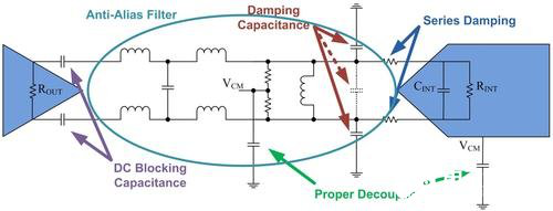
“ADCs with switched-capacitor input sampling networks can also serve as a simple metric when considering noise and other distortions related to the ADC’s analog input and common-mode voltage nodes. Figure 1 shows a typical ADC analog input with integrated driver amplifier and antialiasing filter (AAF).
“
ADCs with switched-capacitor input sampling networks can also serve as a simple metric when considering noise and other distortions related to the ADC’s analog input and common-mode voltage nodes. Figure 1 shows a typical ADC analog input with integrated driver amplifier and antialiasing filter (AAF).
ADC analog input network with integrated amplifier and AAF
Anti-aliasing filters are used to assist with noise and harmonic rejection so that they cannot alias into the frequency bands of interest in other Nyquist zones of the converter. It helps reduce overall system noise and filters any noise that might otherwise couple into the analog input from the rest of the system. The damping capacitor, used in conjunction with the series damping resistor, helps reduce the “backshot” transient current from the ADC switched-capacitor input sampling network.
These components provide a low impedance path that allows these currents to decay between sample clock edges. There are two different ways to implement damping capacitors. It can be a single differential capacitor or split into two single-ended capacitors. There are trade-offs that need to be made based on system requirements. If system cost is critical, then a single capacitor is obviously less expensive. If it is necessary to reduce common-mode noise in the system, two single-ended capacitors may be the best choice.
Often, an easily overlooked part of an analog input network is the common-mode voltage node. In the example of Figure 1, the common-mode voltage levels of the driver amplifier and the ADC are shown to be different at the AC-coupled circuit. This is common because amplifiers require higher supply voltages to maintain proper gain and linearity. Here, it is important to remember that the signal should be routed away from noisy lines and provide proper decoupling. Noise travels all the way to this node and enters the ADC through the VCM output or along the VCM’s connection to the analog input network. Also, care should be taken to decouple at the ADC and also at the connection to the analog input network.
A final piece of advice about the analog input network is to remember to keep the layout of the analog input network symmetrical. Any asymmetry in the analog input network will result in increased even-order distortion of the ADC. This distortion is another form of noise that can degrade ADC performance.
The Links: B150XG01-V8 G121S1-L01


