
Gallium nitride (GaN) replaces silicon to support high-efficiency, high-frequency power supply design
“In all power Electronic applications, power density is one of the key indicators, which is mainly driven by higher energy efficiency and higher switching frequencies. With silicon-based technology approaching its development limit, design engineers are now seeking wide-bandgap technologies such as gallium nitride (GaN) to provide solutions.
“
Author: Yong Ang, Director of Strategic Marketing, ON semiconductor
In all power electronic applications, power density is one of the key indicators, which is mainly driven by higher energy efficiency and higher switching frequencies. With silicon-based technology approaching its development limit, design engineers are now seeking wide-bandgap technologies such as gallium nitride (GaN) to provide solutions.
For new technologies, GaN is inherently cheaper than the technology (silicon) it will replace. GaN devices and silicon devices are produced in the same factory using the same manufacturing process. Therefore, because GaN devices are smaller than equivalent silicon devices, more devices can be produced per wafer, thereby reducing the cost of each wafer.
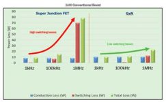
GaN has many performance advantages, including much higher electron mobility than silicon (3.4eV vs. 1.1eV), which gives it the potential for electron conduction efficiency 1,000 times higher than silicon. It is worth noting that the gate charge of GaN (QG) Is relatively low, and because it must be supplemented in each switching cycle, GaN can work at frequencies up to 1 MHz without loss of efficiency, while silicon is difficult to reach above 100 kHz. In addition, unlike silicon, GaN does not have a body diode, and its 2DEG on the AlGaN/GaN boundary surface can conduct current in the opposite direction (referred to as “third quadrant” operation). Therefore, GaN has no reverse recovery charge (QRR), making it very suitable for hard switching applications.
Figure 1: GaN is optimized for fast switching
GaN does have limited avalanche capability and is more susceptible to overvoltage than silicon, so it is extremely suitable for drain-source voltage (VDS) Half-bridge topology clamped to rail voltage. No body diode makes GaN a good choice for hard switching totem pole power factor correction (PFC), and GaN is also very suitable for zero voltage switching (ZVS) applications, including resonant LLC and active clamp flyback.
Fast charging adapters with power levels of 45 W to 65 W will benefit from GaN-based active clamp flyback, while LLC-based GaN is used in high-end laptop power adapters ranging from 150 W to 300 W, such as those used in gaming laptop. In these applications, the use of GaN technology can double the power density, thereby making the adapter smaller and lighter. In particular, related magnetic components can be reduced in size. For example, the size of the power transformer core can be reduced from RM10 to a thin or flat design of RM8. Therefore, in many applications, the power density has doubled or even tripled to 30 W/in3.
In higher power applications, such as power supplies for servers, clouds, and telecommunications systems, especially power supplies based on totem pole PFC, the use of GaN can achieve energy efficiency of more than 99%. This enables these systems to meet the most important (and stringent) energy efficiency standards, such as 80+ titanium.
The method of driving GaN devices is critical to protecting the relatively sensitive gate oxide. It is particularly important to provide an accurately adjusted gate drive amplitude during the on-time of the device. One way to achieve this is to add a low-dropout regulator (LDO) to the existing silicon MOSFET gate driver. But this will damage the gate drive performance, so it is best to use a dedicated half-bridge driver that drives GaN.
More specifically, the typical propagation delay time of a silicon MOSFET driver is about 100 ns, which is not suitable for driving GaN devices with speeds between 500 kHz and 1 MHz. For such speeds, ideally, the transmission delay should not exceed 50 ns.
Due to the low capacitance, there is a high voltage conversion rate between the drain and source of the GaN device. This can lead to premature device failure or even catastrophic failure, especially in high-power applications. To avoid this situation, there must be a high dv/dt immunity (within the range of 100 V/ns).
PCB will have a substantial impact on the performance of GaN designs, so techniques commonly used in RF-type layouts are often used. We also recommend using a low-inductance package (such as PQFN) for the gate driver.
ON Semiconductor’s NCP51820 is the industry’s first half-bridge gate driver, specifically designed for GaN technology. It has a regulated 5.2 V gate drive with a typical propagation delay of only 25 ns. It has a dv/dt immunity of up to 200 V/ns and is packaged in a low-inductance PQFN.
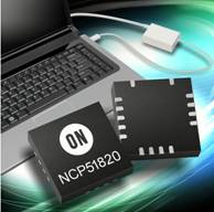
Figure 2: NCP51820 high-performance, 650 V half-bridge gate driver for GaN power switches
The initial use of GaN technology and growth will be applications such as low-power fast-charging USB PD power adapters and high-power adapters for gaming laptops. This is mainly due to the controllers and drivers that can support these applications that require high switching frequencies, thus shortening the design cycle. As suitable driver, controller and module solutions can be used for higher power applications such as servers, cloud and telecommunications, then GaN will also be adopted.
The Links: LQ104S1DG2A TM25T3A-H INFIGBT


