
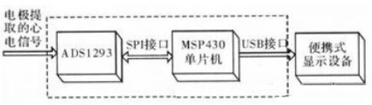
“The ECG signal acquisition system is mainly composed of the signal acquisition front-end ADS1293 and the MSP430 microcontroller control circuit. The working principle is as follows: The human body ECG signal extracted by the electrode is first sent to ADS 1293 for proper amplification and then converted into a digital signal for analog/digital conversion. Then it is sent to the MSP430 microcontroller through the SPI interface for analysis and processing, and finally sent to the portable Display device through the USB interface of the microcontroller to display the waveform in real time.
“
The electrocardiogram is a bioelectrical signal that is generated by the contraction of the heart muscle and can provide information on changes in the physiological function of the heart. The measuring electrodes are placed in different parts of the body, and the potential difference changes on different body surfaces are recorded, and the electrocardiogram is obtained. (Electro Cardio Gram, ECG). It is widely used in clinical medicine due to its easy detection and good intuition. However, the traditional ECG signal acquisition equipment is bulky, and it is inconvenient to acquire ECG signals in real time. Therefore, it is of great significance to study a portable, low-power ECG signal acquisition system. Based on the low-power analog front-end ADS1293, combined with the MSP430 series of low-power microcontrollers, this paper designs an ECG signal acquisition system that can be used for ultra-low power consumption and miniaturization.
1 System hardware design
The ECG signal acquisition system is mainly composed of the signal acquisition front-end ADS1293 and the MSP430 microcontroller control circuit. The working principle is as follows: The human body ECG signal extracted by the electrode is first sent to ADS 1293 for proper amplification and then converted into a digital signal for analog/digital conversion. Then it is sent to the MSP430 microcontroller through the SPI interface for analysis and processing, and finally sent to the portable display device through the USB interface of the microcontroller to display the waveform in real time.

Figure 1 Overall design block diagram of the system
1.1 Signal acquisition front-end ADS1293
The ADS1293 is a Texas Instruments (TI) 3-channel, 24-bit integrated analog front end for biopotential measurements. It can be programmed for each channel for a specific sampling rate and bandwidth, allowing users to customize the performance and power consumption. Optimization. It also has functions such as AC/DC disconnection detection (Lead_off Detect), battery level monitoring and self-diagnosis alarm, and built-in right leg drive circuit rental Wilson/Goldberger terminal required for ECG applications. The connection between the internal structure of ADS1293 and the external pins is shown in Figure 2. From the flow of the signal, it can be divided into signal input interface, signal processing unit and signal output interface.
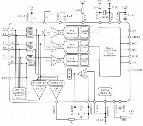
Figure 2 Schematic diagram of ADS1293
(1) Signal input interface. There are 6 signal input pins from IN1 to IN6, and all input pins include an electromagnetic interference (EMI) filter to filter out radio frequency noise. The system adopts a 5-lead connection mode, that is, the right arm (RA), left arm (LA) and left leg (LL) are connected to IN1, IN2 and IN3 pins respectively; the common mode detector (CM detect) obtains RA, LA and The average voltage of LL is used as the input of the right leg drive (RLD) amplifier, and the output of the right leg drive amplifier is returned to the right leg (RL) terminal, together with the input from the IN4 pin. The function of the right leg drive circuit is to control the common mode level of the patient and improve the AC rejection ratio of the system; the output of the Wilson network (WCT) is connected to the IN6 pin, which together with the V1 (chest electrode) connected to the IN5 pin is used as the CH3 channel differential signal input.
(2) Signal processing unit. It is mainly composed of instrument amplifier (INA), Σ△ regulator (SDM) and low-pass digital filter (Digital Filter), and its main function is to convert differential analog voltage signals into digital signals. The instrumentation amplifier is an operational amplifier circuit with high input impedance. It has two main functions: 1) It can amplify the differential signal to a certain extent. 2) Provides high input impedance in order to obtain a larger input signal from the ECG electrodes. The output signal of the instrumentation amplifier is sent to the ΣΔ modulator for analog-to-digital conversion. The ΣΔ modulator is a one-bit encoding technology based on oversampling, and outputs a one-bit encoded data stream that reflects the amplitude of the input signal. The low-pass digital filter is composed of three programmable 5th-order sin-type filters. After the output of the ΣΔ modulator is processed by the low-pass digital filter, the N-bit encoded output can be obtained.
(3) Signal output interface. It mainly includes 4-wire SPI serial interface, DRDYB pin and ALRAM pin. The functions of each pin are as follows: SCLK is the serial clock input pin; SDI is the serial data input pin, with a total of 16 bits, including 1-bit read-write control, 7-bit address and 8-bit data. During the rising edge of the clock, all data is sampled and written to the register on the 16th rising edge of the clock. SDO is the serial data output pin, at 8~15 clock falling edges, the SDO pin reads data. CSB is the chip select pin, low level is active, the SPI interface starts to read and write data during the low level, and the low level is maintained for 16 clock cycles; DRDYB is the end pin of analog-to-digital conversion, indicating that the data inside the chip is ready Can be read, active low, usually used as CPU interrupt signal or status query signal; ALARMB is an alarm pin, ADS1293 has a self-diagnosis alarm system for diagnosing abnormal conditions that may occur in ECG applications, these Abnormal conditions mainly include electrode falling off, synchronization error, low power warning and abnormal operation of 3 channels, etc. Once an abnormal condition occurs, it will be reported to the error flag and displayed on the ARLAM pin.
1.2 MSP430 microcontroller control circuit
Select TI’s ultra-low power microcontroller MSP430F5529 as the main controller, which has a wealth of on-chip peripherals, and each module runs completely independently, including timers, input/output ports, watchdog and UART, etc. All can sleep in the main CPU operate independently in the state. With all modules active, the current is typically 290µA/MHz. In standby mode, the typical value of the current is only 0.18μA, and the response time from standby to wake-up is 3.5μs. The MSP430F5529 contains 2 Universal Serial Communication Interface (USCI) modules that support multiple communication modes such as UART, IrDA, I2C, SPI and USB. In the system, MSP430F5529 uses SPI interface to control and transmit data to ADS1293. Among them, MSP430F5529 works in master mode and ADS1293 works in slave mode. Transfer data to portable display device or computer through USB interface, Figure 3 shows the interface circuit of MSP430F5529.
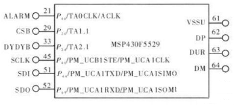
Figure 3 MSP430 microcontroller interface circuit
2 System software design
The system software mainly includes: (1) Control the ADS1293, complete the analog/digital conversion of the ECG signal, and read the data through the SPI interface. (2) The data is transmitted to the display device for real-time display through the USB interface, and the program flow is shown in Figure 4.
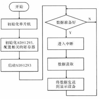
Figure 4 Program flow chart
First, initialize the microcontroller, configure the SPI interface that communicates with the ADS1293 and the USB interface that connects with the display device. Then, the initialization of the ADS1293 is realized by setting the relevant registers, including the setting of the operating frequency of the instrumentation amplifier and the ΣΔ regulator, the parameter setting of the programmable filter, and the setting of each alarm register. Then start the ADS1293, and judge whether the ADS1293 analog/digital conversion is completed and whether the data is ready by querying the state of the DRDYB pin. If not, continue to query. Otherwise, generate an interrupt to the microcontroller MSP430F5529 and then read the data in the ADS1293 register through the SPI interface, and send it to the display device through the USB interface.
3 Conclusion
This paper proposes a design method for a low-power, portable ECG signal acquisition system. The system uses the low-power analog front-end chip ADS1293 to replace the traditional discrete front-end circuit, and uses the modules required for ECG applications such as the right leg drive circuit, Wilson terminal, and electrode drop detection integrated in the ADS1293 to simplify the front-end circuit. Compared with the conventional solution, the number of components can be reduced by more than 90%. The ADS1293 consumes only 0.3 mW per channel and has flexible power down and standby modes to extend battery life in portable devices. To sum up, the system has the advantages of low power consumption and small size, and has a wide application prospect.
The Links: 1MBI600PX-120 SKM400GA123D


