
The crystal oscillator also has to look at how to design PCB crystal oscillators
“Jingzhen, a common topic. In previous articles, the editor explained various aspects of crystal oscillators, such as which crystal oscillators are equipped on the PCB. In this article, I will discuss with you how to design PCB crystal oscillators.
“
Jingzhen, a common topic. In previous articles, the editor explained various aspects of crystal oscillators, such as which crystal oscillators are equipped on the PCB. In this article, I will discuss with you how to design PCB crystal oscillators.
We often compare the crystal oscillator to the heart of the digital circuit. This is because all the work of the digital circuit is inseparable from the clock signal. The crystal oscillator directly controls the entire system. If the crystal oscillator does not work, the entire system will be paralyzed, so the crystal oscillator is the decision The prerequisites for the digital circuit to start working.
The crystal oscillators we often talk about are quartz crystal oscillators and quartz crystal resonators, both of which are made using the piezoelectric effect of quartz crystals. Applying an electric field on the two electrodes of a quartz crystal will cause mechanical deformation of the crystal. On the contrary, if mechanical pressure is applied on both sides of the crystal, an electric field will be generated on the crystal. Moreover, these two phenomena are reversible. Using this feature, applying alternating voltage on both sides of the crystal, the wafer will generate mechanical vibrations and at the same time generate an alternating electric field. This kind of vibration and electric field are generally very small, but at a certain frequency, the amplitude will increase significantly. This is piezoelectric resonance, which is similar to the common LC circuit resonance.
As the heart of the digital circuit, how does the crystal oscillator play a role in smart products? For smart home products such as air conditioners, curtains, security, monitoring, etc., wireless transmission modules are required, and they use protocols such as Bluetooth, WIFI or ZIGBEE , Send the module from one end to the other, or directly control it through the mobile phone. The crystal oscillator is the core component of the wireless module, which affects the stability of the entire system. Therefore, the choice of the crystal oscillator used in the system determines the success or failure of the digital circuit.
Due to the importance of crystal oscillators in digital circuits, we need to be careful when using and designing:
1. There is a quartz crystal inside the crystal oscillator, which will easily cause the quartz crystal to break and break when it is subjected to external impact or fall, which will cause the crystal oscillator to fail to vibrate. Therefore, the reliable installation of the crystal oscillator should be considered when designing the circuit. Wait.
2. Pay attention to the welding temperature during manual welding or machine welding. The crystal oscillator is sensitive to temperature. The temperature should not be too high during soldering, and the heating time should be as short as possible?
Reasonable crystal oscillator layout can suppress system radiation interference
1. Problem description
This product is a field camera, which is composed of five parts: core control board, sensor board, camera, SD memory card and battery. The outer shell is a plastic shell. The small board has only two interfaces: DC5V external power interface and USB interface for data transmission. After radiation test, it is found that there is a problem of harmonic noise radiation around 33MHz.
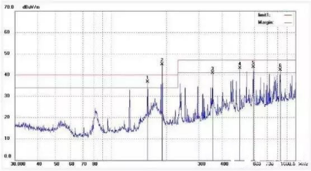
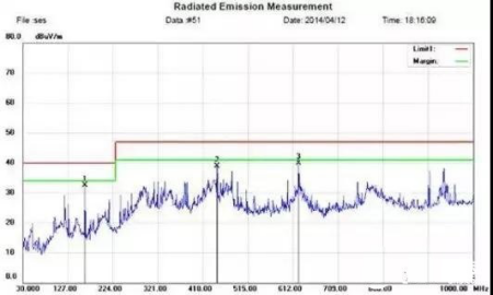
The original test data is as follows:
2. Analyze the problem
The shell structure of this product is made of a non-shielding material. Only the power cord and USB cable lead out of the shell in the whole machine test. Is the interference frequency radiated by the power cord and USB cable? So the following tests were performed separately:
(1) Only add a magnetic ring to the power line, the test result: the improvement is not obvious;
(2) Only add a magnetic ring to the USB cable, the test result: the improvement is still not obvious;
(3) A magnetic ring is added to both the USB cable and the power cable. The test result: the improvement is obvious, and the overall interference frequency is reduced.
It can be seen from the above that the interference frequency is brought out from the two interfaces. It is not the problem of the power interface or the USB interface, but the internal interference frequency is coupled to these two interfaces. It cannot be solved by shielding only one interface. problem.
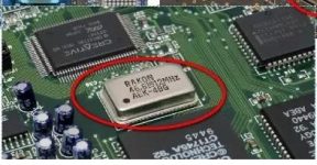
After near-field measurement, it is found that the interference frequency comes from a 32.768KHz crystal oscillator of the core control board, which produces strong spatial radiation, which makes the surrounding traces and GND coupled with 32.768KHz harmonic noise, and then through the interface The USB cable and the power cable are coupled and radiated. The problem with this crystal is caused by the following two problems:
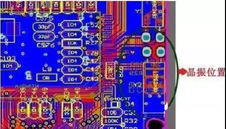
(1) If the crystal oscillator is too close to the edge of the board, it is easy to cause the crystal oscillator to radiate noise.
(2) There are signal lines under the crystal oscillator, which easily causes the signal line to couple the harmonic noise of the crystal oscillator.
(3) The filter device is placed under the crystal oscillator, and the filter capacitor and matching resistor are not arranged according to the signal flow direction, which makes the filtering effect of the filter device worse.
Three, the solution
According to the analysis, the following countermeasures are drawn:
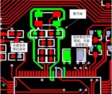
(1) The filter capacitor and matching resistor of the crystal should be placed close to the CPU chip first, away from the edge of the board;
(2) Remember not to place the ground in the crystal placement area and the projection area below;
(3) The filter capacitor and matching resistance of the crystal are arranged according to the signal flow direction, and they are placed neatly and compactly near the crystal;
(4) Place the crystal close to the chip, and the wiring between the two should be as short and straight as possible.
You can refer to the layout as shown below:
After rectification, the prototype test results are as follows:
4. Conclusion
Nowadays, many system crystal oscillators have high clock frequency and strong interference harmonic energy; interference harmonics are not only conducted from the two traces of its input and output, but also radiated from space. If the layout is unreasonable, it is easy to cause strong The problem of noise radiation is difficult to solve by other methods, so the layout of the crystal oscillator and CLK signal line is very important in the PCB layout.
PCB design considerations for crystal oscillators
(1) Coupling capacitors should be placed as close as possible to the power pin of the crystal oscillator, and the order of placement: according to the direction of the power supply, place them in descending order of capacitance value, and the capacitor with the smallest capacitance value is closest to the power pin.
(2) The shell of the crystal oscillator must be grounded, which can radiate the crystal oscillator to the outside, and can also shield the interference of external signals to the crystal oscillator.
(3) Do not wire under the crystal oscillator, ensure that the ground is completely laid, and do not wire within the 300mil range of the crystal oscillator, so as to prevent the crystal oscillator from interfering with the performance of other wiring, devices and layers.
(4) The trace of the clock signal should be as short as possible and the line width should be larger. Find a balance between the length of the wiring and the distance from the heat source.
(5) Do not place the crystal oscillator on the edge of the PCB board. Pay special attention to this point when designing the board.
The Links: 6MBP75RS120 IP4283CZ10-TBA ELE INSTOCK


