

“Today, embedded vision system designers need to cater to many market trends. For example, more and more sensors are used in current designs, making it easier to collect more data or implement new functions. For example, in the automotive market, a few decades ago, car manufacturers installed a backup camera on their vehicles is considered an innovation, but now they have begun to use the camera for road deviation monitoring, speed sign recognition and many other intelligent driving applications.
“
Today, embedded vision system designers need to cater to many market trends. For example, more and more sensors are used in current designs, making it easier to collect more data or implement new functions. For example, in the automotive market, a few decades ago, car manufacturers installed a backup camera on their vehicles is considered an innovation, but now they have begun to use the camera for road deviation monitoring, speed sign recognition and many other intelligent driving applications.
At the same time, embedded vision system designers are gradually adopting components that comply with the Mobile Industry Processor Interface (MIPI) Alliance standards. MIPI was originally developed for the mobile market. It defines the hardware and software interface standards required by mobile device designers to build high-performance, cost-effective, and reliable mobile solutions. In the past few years, MIPI has become the mainstream standard for developing embedded systems. Designers of various applications including industry and automobiles have realized this and have begun to find ways to take advantage of the high performance and economies of scale of mobile components.
The pressure to shorten time to market has also driven the demand for easy-to-use embedded vision solutions. It is no longer enough to only provide chips. These pressures make designers urgently need an embedded vision design environment that can provide all hardware, software, IP, and reference designs to quickly design and develop end products. At the same time, today’s users expect their embedded displays to be as responsive as consumer electronics. Embedded displays that start slowly can introduce artifacts and ruin the user experience.
new challenge
While these fast-developing trends create opportunities, they also bring severe challenges to embedded vision designers. First, the cameras and displays used in many embedded systems do not match the type or number of interfaces of today’s application processors (AP). The I/O used for sensors on the AP is very limited, but it has to support various displays and sensors. What’s more difficult is that the Display sizes and resolutions of various applications are not the same. In addition, industrial displays have a long service life, and many displays that are still in use were initially connected through traditional interfaces. So, when designers of embedded applications have to use traditional or dedicated displays and sensors in their designs, how can they make good use of the advantages of the MIPI component market?
In order to support the use of more sensors and more effective management of I/O resources, designers need programmable solutions to make up for the lack of I/O. Ideally, such a solution needs to aggregate sensor inputs and allow designers to preprocess the data to reduce the load on the processor. The ideal solution also needs to be programmable and able to easily adapt to a customized display design. In the past, designers could only support different display sizes and resolutions by developing specialized ASICs for each display type. The programmable solution can use a single device to achieve different display requirements.
In 2016, with the introduction of the CrossLinkTM series of FPGAs, Lattice semiconductor became a supplier in this field. This is a programmable video bridge device that supports various protocols and interfaces for connecting mobile image sensors and display screens. In order to meet the growing demand of the embedded video market, Lattice has introduced an enhanced version of CrossLink-CrossLinkPlusTM. CrossLinkPlus has added a 2 Mbit embedded flash memory as a configuration memory to meet the needs of users for seamless startup of the display. With the on-chip flash memory, CrossLinkPlus can be started instantaneously within 10ms, while the human brain generally cannot perceive the image within 15ms, so there will be no artifacts that interfere with the user experience. On-chip flash memory can support on-site reprogramming.

Figure 1: CrossLinkPlus FPGA from Lattice Semiconductor
CrossLinkPlus has the fast MIPI D-PHY in the FPGA of the same size, and the power consumption is very low. This FPGA package size is only 3.5 x 3.5 mm and supports a total of 12 Gbps D-PHY. In addition to high-speed MIPI D-PHY, CrossLinkPlus also has a 6K LUT programmable FPGA architecture and flexible high-speed I/O, and supports video bridging of MIPI CSI-2, MIPI DSI, LVDS, SLVS200, CMOS and Sub-LVDS interfaces. Because CrossLinkPlus can connect to such displays and sensors, it provides design teams with great design flexibility.
The new device can help the development team to improve the design efficiency, so as to deal with the pressure of the product to market quickly. For example, ready-to-use pre-verified IP libraries for functions such as receivers, converters, and transmitters allow designers to focus on developing the high-value features of their designs, allowing their products to stand out from the competition. Pre-verified video IP modules and reference designs not only shorten the design cycle, they can also be obtained immediately. In addition, these IP modules can be reused in CrossLink and CrossLinkplus product series.
Lattice also provides easy-to-use hardware and software tools to simulate functional performance, verify system-level functions, and accelerate product development. The embedded flash memory on the device allows designers to update the bit stream in the field to meet changing market demands. The new CrossLinkPlus can also help engineers solve strict size and power consumption constraints, while avoiding the use of external flash memory to generate more power consumption.
From a competitive point of view, the hard-core MIPI D-PHY rate per unit size of this device is the fastest in the industry. Compared with similar competitors, Lattice CrossLinkPlus is not only smaller in size, but also has stronger D-PHY performance and lower power consumption.

Figure 2: Lattice CrossLinkPlus FPGA not only provides high-performance MIPI D-PHY, but also extremely low power consumption
Lattice provides extensive support for accelerating product development. For example, Lattice regularly releases new reference designs based on CrossLink and CrossLinkPlus. These reference designs are customized to implement popular video bridging features on new or existing product designs.
New application
Common use cases of CrossLinkPlus show that it can give designers a high degree of design flexibility. Figure 3 below describes how to use this device to bridge sensors and processors with different interfaces. Here, designers face such a problem: On the one hand, they want to take advantage of the cost, performance, and size of the MIPI processor; on the other hand, they want to keep the existing cameras that use industry standards. In the machine vision application of Figure 3,
Designers use CrossLinkPlus to bridge the Sub-LVDS interface camera and the D-PHY interface MIPI processor.
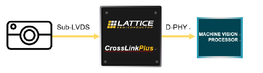
Figure 3: In this application example, the Lattice CrossLinkPlus FPGA acts as a bridge between the Sub-LVDS camera and the MIPI I/O of the machine vision processor.
The second potential application of Lattice CrossLinkPlus is to aggregate the input of multiple sensors and send it to the application processor. For example, in Figure 4, three image sensors are connected to the CrossLinkPlus device through three D-PHY ports. CrossLinkPlus aggregates sensor data and outputs it to the processor through a single D-PHY. Designers can use this aggregation function to optimize the use of the processor’s limited I/O resources.
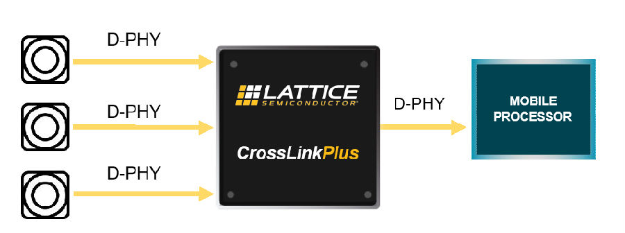
Figure 4: Lattice CrossLinkPlus can aggregate multiple sensor signals on one port, saving processor I/O
Designers can also use CrossLinkPlus to realize MIPI signal separation or replication. In Figure 5, the designer feeds the signal from the sensor into the CrossLinkPlus device, and then splits the output or copies it into two separate outputs. Lattice believes that this approach will be increasingly used in ADAS for smart cars or applications that focus on data redundancy. Here, the signal from the camera enters the Lattice CrossLinkPlus device and is copied to two output streams. An application processor that is sent to process the data in real time. The second is archived locally or in the cloud for data recording and backup, similar to the black box of an airplane. In the event of a malfunction or a traffic accident, investigators can view the data backup to determine the cause of the accident.
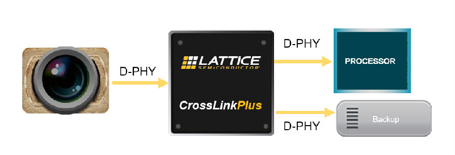
Figure 5: In this ADAS vision system, CrossLinkPlus FPGA replicates the camera signal output and sends it to the application processor and data backup place
Figure 6 below shows how designers use CrossLinkPlus to connect traditional displays to a new high-performance AP. Many industrial control applications need to use bridge devices when connecting traditional displays and APs with OpenLDI interfaces, because OpenLDI displays are usually much larger than MIPI displays. The new MIPI application processor transmits data to CrossLinkPlus via D-PHY. Then, the device uses the OpenLDI bridge to send the data to the traditional display. Similarly, CrossLinkPlus can be used to bridge non-MIPI interface image sensors and MIPI APs.
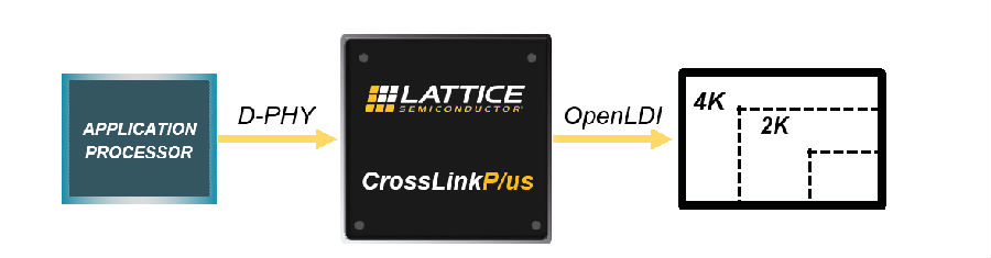
Figure 6: In this application example, Lattice CrossLinkPlus realizes the connection between a traditional display and a modern application processor
in conclusion
Now, with Lattice CrossLinkPlus, designers who want to speed up embedded vision development don’t have to look for it. By introducing the reprogrammability of FPGAs into embedded vision systems, CrossLinkPlus allows designers to take advantage of the cost and performance advantages provided by MIPI components. Its hard core D-PHY interface can provide industry performance, and embedded flash memory can realize instantaneous display. The device has extremely low operating power consumption and small size, which helps to simplify heat dissipation management, and its support for various commonly used interfaces and traditional interfaces improves design flexibility to a limited extent. CrossLinkPlus’ comprehensive, pre-verified and IP library further accelerates the development speed, allowing designers to spend more time on the part of the design-enhancing the competitive advantage.
The Links: DG32240-17 2MBI600VD-060-50


