
[Guide]In the previous article, we introduced the control circuit of the “Power Sequence Specification ①” of the power sequence control circuit using a universal power IC. This article first introduces the use of universal power IC to realize the power sequence control circuit, the sequence work when the power is turned on.
Power sequence specification ①: sequence work when the power is on
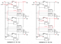
As introduced in the previous article, the sequence of specification ① is to output the three systems of 1.2V, 3.3V, and 1.5V in sequence. The sequence work will be described in order below. In the introduction, the operation of applying 1.2V is described as the “first stage”, the operation of applying 3.3V is described as the “second stage”, and the operation of applying 1.5V is described as the “third stage”, and the three systems The state of both conducting is expressed as “when the power supply is working”. In the diagrams of each stage, the parts corresponding to the description are shown in red.
v In the initial state, the Enable pin is at “L” level, and the three DCDC outputs are all zero.
Work when the power is turned on in the first stage
1) Set the Enable pin to “H” level to start the power supply.
2) Since the EN pin of DCDC 1 becomes “H” through diode D1, DCDC 1 is activated.
3) When the output voltage of DCDC 1 rises from 0V to 1.2V, the output of Power Good 1 changes from “L” level to “H” level, and the EN pin of the next stage of DCDC 2 becomes “H” Level.
4) The IN pins of Power Good 3 and Power Good 4 are given “H” level by diodes D2 and D4, so the PGOOD pin (output) maintains high impedance.

Work when the power is turned on in the second stage
1) The EN pin of DCDC 2 becomes “H” level, so DCDC 2 starts.
2) When the output voltage of DCDC 2 rises from 0V to 3.3V, the output of Power Good 2 changes from “L” to “H”, and the EN pin of the next stage DCDC 3 changes to “H”.
Work when the power is turned on in the third stage
1) The EN pin of DCDC 3 becomes “H” level, so DCDC 3 is activated.
2) The output voltage of DCDC 3 rises from 0V to 1.5V. At this point, the power supplies of the three systems are all in working state (see the separate diagram for the main node states when the power is working).

In the next article, we will introduce the timing operation during turn-off.
Key points
・In the sequence ①, the sequence of turning on the power of the three systems in order and turning off in the reverse order is realized.
・In order to understand the timing operation, this article lists the operation diagrams of the three systems when the power is turned on.
The Links: 2SAR533P5T100 LTM170E8-L03


