
Design of Data Acquisition and Processing System Based on TMS320C6203B and CY7C68013 Chips
“With the continuous development of digital signal processing theory and computer, modern industrial production and scientific and technological research need to rely on digital processing methods. The prerequisite for digital processing is to digitize the research object, so the technology of data acquisition and processing has been paid more and more attention. In some fields such as image processing, transient signal detection, software radio, etc., data acquisition and processing technology with high speed, high precision and high real-time performance is required. Today’s high-speed data acquisition and processing cards generally use the framework of high-performance digital signal processors (DSP) and high-speed bus technology.
“
Authors: Huang Hu, Zhou Yunshan, Yi Wen
With the continuous development of digital signal processing theory and computer, modern industrial production and scientific and technological research need to rely on digital processing methods. The prerequisite for digital processing is to digitize the research object, so the technology of data acquisition and processing has been paid more and more attention. In some fields such as image processing, transient signal detection, software radio, etc., data acquisition and processing technology with high speed, high precision and high real-time performance is required. Today’s high-speed data acquisition and processing cards generally use the framework of high-performance digital signal processors (DSP) and high-speed bus technology.
DSP is used to complete real-time processing algorithms with huge computational load, and high-speed bus technology completes the fast transmission of processing results or sampled data. DSP mainly adopts the products of TI or ADI Company, and the high-speed bus can adopt ISA, PCI, USB and other bus technologies. At present, the PCI bus is widely used. Although it has many advantages, it has the following serious defects; it is easily affected by the environment inside the chassis, and it is impossible to connect many devices due to the limitation of the address of the number of computer slots and interrupt resources, etc. .
The USB bus has the advantages of convenient installation, high bandwidth, and easy expansion. Among them, the USB2.0 standard has a transmission rate of up to 4800bps, and has gradually become the mainstream of computer interfaces. This paper introduces a high-speed data acquisition and processing system using USB2.0 interface and high-performance DSP, which is mainly designed for wavelength detection and adjustment of dense wavelength division multiplexing system in optical fiber communication, and can also be applied to image processing, radar signal processing and other related fields.
1 Principle of high-speed data acquisition and processing system and device selection
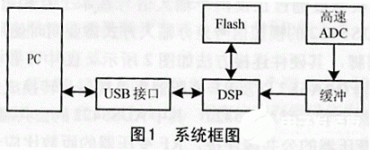
The hardware composition of the whole high-speed data acquisition and processing system is: high-speed ADC, high-speed large-capacity data buffer, high-performance DSP and USB2.0 interface. The principle block diagram of the system is shown in Figure 1.
The high-performance DSP adopts TMS320C6203B in TI’s TMS320C6000 series fixed-point DSP; the high-speed ADC adopts TI’s ADS5422, 14-bit sampling, and the maximum sampling frequency is 62MHz; the PC interface adopts USB2.0, and the theoretical maximum data transmission rate is 480Mbps. The CY7C68013 in the EZ-USB FX2 series of Cypress Company is selected; the data buffer adopts the high-speed and large-capacity FIFO device IDT72V2113 of IDT Company; the program is stored in the Flash memory, and the device adopts SST291E010. The main features of each device are introduced one by one below.
(1) TMS320C6203B
TMS320C6203B is a kind of high-performance digital signal processor TMS320C6000 series of TI company in the United States. It adopts the modified Harvard bus structure and has a set of 256-bit program bus, two sets of 32-bit program bus and a set of 32-bit DMA dedicated bus; There are 8 functional units inside that can operate in parallel, the maximum operating frequency is 300MHz, and the maximum processing capacity is 2400MIPS; it integrates peripheral device interfaces, such as external memory interface (EMIF), external expansion bus (XB), multi-channel buffer serial port (McBSPs) ) and a host interface (HPI) for easy connection to external memory, coprocessors, hosts, and serial devices.
(2) ADS5422
ADS5422 is a high-speed parallel 14-bit analog-to-digital converter produced by TI Company in the United States. Its maximum sampling frequency reaches 62MHz. When the sampling frequency is 100MHz, the SNR is 72dB and the SFDR is 85dB. The analog signal input can be single-ended input or differential input. The maximum input signal peak-to-peak value is 4V, and a single 5V power supply is supplied. The output digital signal is fully compatible with 3.3V devices, and provides a full-scale mark of the input signal and a valid mark of the output digital signal, which facilitates connection with other devices.
(3) IDT72V2113
IDT72V2113 is a high-speed large-capacity first-in first-out memory device (FIFO) produced by IDT Corporation of the United States. Its maximum operating frequency is 133MHz; the capacity is 512KB, and the capacity can be easily set to 512K×9bit or 256K×18bit through pins; IDT72V2113 can set standard working mode or FWFT (First Word Fall Through) working mode, and Provides five signs of full, half full, full empty, near full and near empty; very convenient for capacity expansion. Capacity expansion is a major feature of IDT72V2113. The expansion methods can be divided into word length expansion and word depth expansion. Through easy expansion, it can be buffered with larger capacity in the form of multiple pieces of IDT72V2113, and the circuit connection is simple and reliable.
(4) CY7C68013
CY7C68013 is a USB2.0 chip launched by Cypress Company of the United States. It is a fully integrated solution, which takes up less circuit board space and shortens development time. The main structure of CY7C68013 is as follows: including 1 8051 processor, 1 intelligent serial interface engine (SIE), 1 USB transceiver, 16KB on-chip RAM (including 4KB FIFO) memory to host 1 general programmable interface (GPIF) .
The unique architecture of CY7C68013 has the following characteristics:
①Including an intelligent serial interface engine (SIE), which performs all basic USB functions, liberates the embedded MCU to realize other rich functions, to ensure continuous high-speed and effective data transmission;
②The large-capacity FIFO with 4KB is used for data buffering. When used as a slave device, the Synchronous/Asynchronous FIFO interface can be used to connect with the master device (such as ASIC, DSP, etc.); when used as a master device, it can be connected through a general programmable interface ( GPIF) in the form of arbitrary control waveforms to achieve connection with other slave devices, which can easily be compatible with most bus standards, including ATA, UTOPIA, EPP and PCMCIA, etc.;
③ Firmware software configuration, the firmware that needs to be run on CY7C68013 can be stored on the host, and when the USB device is connected to the host, it can be downloaded to the device, so that the firmware can be easily modified without changing the hardware;
④ It can fully realize the USB2.0 (version 2000) protocol and is backward compatible with USB1.1.
2 Hardware connection of high-speed data acquisition and processing system
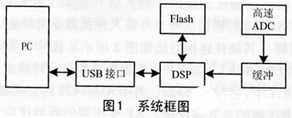
2.1 Analog signal input circuit
The analog signal input of ADS5422 can adopt single-ended input mode or differential input mode. The single-ended input method is relatively simple to connect, but the anti-noise performance is poor, so we adopt the differential input method to minimize signal noise and electromagnetic interference, especially the differential input method can input all even-order harmonics through the positive and negative input. The signals basically cancel each other out.
The analog signal differential input method of ADS5422 needs to use IN and IN pins at the same time, and its hardware connection method is shown in Figure 2. In the figure, first use the amplifier OPA687 and the RF transformer to convert the single-ended signal into a differential signal, and then input it to the ADS5422, where the common terminal CM of the ADS5422 is connected to the common terminal of the RF transformer, and the turns ratio of the RF transformer should be determined according to the signal. In order to enhance the stability of the signal, an RC low-pass filter circuit is added before the input of each signal of the ADS5422. In Figure 2, it is recommended that Rt be 50Ω, Rin is 22Ω, and Cin is 10pF. These components can also be adjusted according to specific signals. Under normal circumstances, the resistance value is between 10 and 100Ω, and the capacitance value is between 10 and 200pF.
2.2 Connection between ADS5422 and IDT72V2113
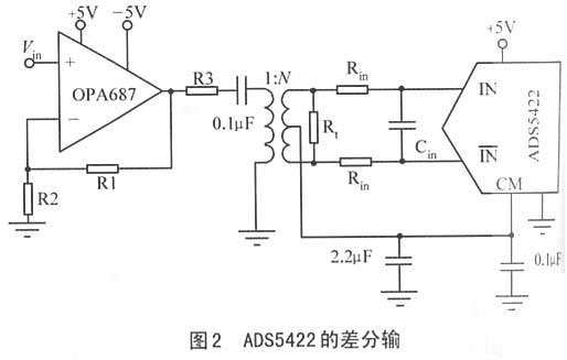
Although the power supply voltage of ADS5422 is 5V, the digital signal level it outputs is compatible with 3.3V level, so no level conversion chip is required, just connect the data line of ADS5422 to the data line of IDT72V2113. However, the ADS5422 samples and stores the sampled data in the IDT72V3113. These two operations have very strict timing configuration requirements. If the timing relationship between the two is not well matched, data storage errors or data loss will occur. How to realize sampling and storage simply and reliably is the difficulty in designing this part of the circuit. The general method is to realize the timing between the ADC and the FIFO memory through a programmable logic device (CPLD or FPGA), that is, the CPLD or FPGA controls the ADC sampling and the write operation of the FIFO memory. However, by carefully looking at the working timing diagrams of ADS5422 and IDT72V2113, a simple and reliable implementation method has been found, which does not require CPLD or FPGA to achieve timing coordination between the two.
First analyze the working timing diagram of ADS5422, as shown in Figure 3, where t1 is the time interval between the upper edge of the sampling clock and the invalidation of the output data, that is, the data retention time, and its size is 3ns. Looking at the relevant documents of IDT72V2113, it can be seen that when writing to it, the holding time of the data line is greater than 1ns to meet the requirements. Therefore, the timing coordination between ADS5422 and IDT72V2113 can be implemented in the following simple ways: the sampling clock of ADS5422 and the write clock of IDT72V2113 use the same clock source, so that on the rising edge of each clock, ADS5422 performs analog-to-digital conversion, and at the same time Store the sampled data output in the last clock cycle into the DT72V2113.
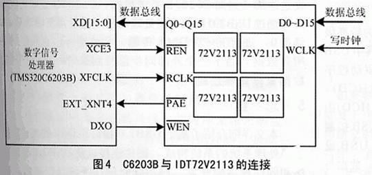
2.3 Connection between C6203B and IDT72V2113
The connection between C6203B and IDT72V2113 is through C6203B external expansion bus (XB). The external expansion bus (XB) of C6203B is 32 bits wide, which can realize seamless connection with synchronous FIFO, and can realize four FIFO write interfaces or three FIFO write interfaces and one FIFO read interface seamlessly at the same time. The FIFO read interface is realized through seamless connection. The FIFO must be connected to the XCE3, and the data is transferred from the IDT72V2113 to the on-chip RAM of the C6203B through DMA. The specific connection is shown in Figure 4. In Figure 4, 4 pieces of IDT72V2113 are expanded by word length and word depth to form a 2MB data input buffer, input data bus (D0~D15), output data bus (Q0~Q15), read enable (REN), read clock (RCLK) ), write enable (WEN), write clock (WCLK) and empty flag signal (PAE) are formed by the corresponding signal combination of 4 pieces of IDT72V2113; XCE3 is the space selection signal of the external expansion bus (XB), XFCLK is the external The output clock of the expansion bus (XB), EXT_INT4 is the external interrupt signal 4 of C6203B, and DX0 is used as a general output port to control the write enable signal of IDT72V2113.
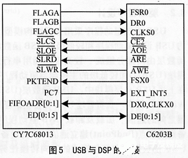
2.4 Connection between CY7C68013 and C6203B
3 USB software design
A considerable amount of work in the development of USB interface is about the development of USB software. USB software includes three aspects of work: firmware (firmware) design, driver design and host-side application design.
3.1 Firmware Design
Firmware is a program running on CY7C68013, which can be designed in assembly language or C language. Its main function is to control CY7C68013 to receive and process requests from USB drivers (such as requesting device descriptors, requesting or setting device status, requesting or setting device interface) Waiting for USB2.0 standard request), control CY7C68013 to receive application control instructions, store data through CY7C68013 and upload it to PC in real time, etc.
The firmware design ideas in this solution are as follows:
①Make CY7C68013 work in asynchronous slave FIFO (Asynchronous Slave FIFO) mode. The corresponding register operation is: IFCONFIG=0xCB.
CY7C68013 has a variety of working modes. In addition to being a master control chip capable of generating arbitrary control waveforms, even as a slave device, asynchronous or synchronous modes can be selected. Due to the relationship of DSP, this scheme chooses the asynchronous slave mode.
② The 4KB FIFO corresponds to two endpoints (EndPoint), namely EndPoint2 and EndPoint6. The corresponding register operation is: EP2CFG=0xA0, EP6CFG=0xF2.
EndPoint2 and EndPoint6 correspond to 2KB built-in FIFOs (hereinafter referred to as FIFO2 and FIFO6 respectively), which store the data that the USB needs to upload and receive. Among them, EndPoint2 is an OUT type, which is responsible for receiving data from the host; EndPoint6 is an IN type, which is responsible for sending data to the host. In addition, both EndPoint2 and EndPoint6 adopt the bulk (BULK) transmission method. Compared with other transmission methods defined by USB2.0, this method has the characteristics of reliable data and high transmission rate, and is the most commonly used transmission method.
③ Configure the FIFO. The corresponding register operation is: EP2FIFOCFG=0x11, EP6FIFOCFG=0x0D.
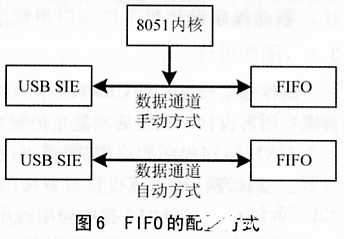
In this scheme, FIFO2 and FIFO6 are set to automatic mode. The so-called “automatic” here means that the 8051 core of CY7C68013 does not need to participate in the data transmission process. If there are special needs, it can be set to manual mode, so that the 8051 can modify the data, as shown in Figure 6. In addition, the FIFO is configured as a 16-bit interface.
④Other operations. In order to improve the entire USB transmission function and improve the robustness of the firmware, other designs must be matched, including functions such as automatic FIFO clearing and reset, personalized commands, etc., which will not be discussed in detail here.
3.2 Driver Design
The USB system driver adopts a hierarchical structure model, which is a higher-level USB device driver and a lower-level USB function layer. The USB function layer consists of two parts: a higher-level Universal Serial Bus driver module (USBD) and a lower-level host controller driver module (HCD). In the above-mentioned USB layered module, the USB function layer (USBD and HCD) is provided by Windows, which is responsible for managing the communication between the USB device driver and the USB controller; loading and unloading the USB driver; and the USB device common endpoint (EndPoint) Establish communication and perform bidirectional conversion tasks of device configuration, data and USB protocol frame and packaging format. At present, Windows provides a variety of USB device drivers, but not for real-time data acquisition devices, so the USB device driver needs to be written by the developer.
To develop USB device drivers, the development kit Driver Works of Numega and 2000DDK of Microsoft can be used, and VC++6.0 is used as an auxiliary development environment. The driver wizard provided by Driver Works can automatically generate the code framework according to the needs of users, which reduces the difficulty of development and shortens the development cycle. However, in order to facilitate the user to develop the USB interface, Cypress provides a general driver in the development kit of CY7C68013, which can be used directly after being compiled by DDK without modification. In this design scheme, this general driver is used.
3.3 Application Design
The host application program mainly realizes fetching the processed data from the high-speed data acquisition and processing board, storing and displaying the processing structure, and sending control commands to the data acquisition and processing board. Under Windows 2000, the application development tool we use is VC++6.0.
4 How the system works
After power-on, ADS5422 works all the time, and whether the data generated by sampling is stored in IDT72V2113 is determined by the DX0 pin state of C6203B. The C6203B is initialized, and the XCE3 of the external expansion bus is set to the synchronous FIFO read operation mode. DMA channel 0 is configured to transmit 1 frame at a time, with 1024 half-words per frame, the synchronization event is set to external interrupt 4, the trigger polarity is high level, the timer 0 is initialized, and the timing interval is 22ms. When the external synchronization signal comes, start timer 0, manually start DMA channel 0, and set DX0 to low level at the same time.
The data generated by ADS5422 sampling begins to be written into IDT72V2113. When the timer 0 interrupt arrives, set DX0 to high level, turn off the write enable of IDT72V2113, and the sampled data is no longer stored in IDT72V2113. As the data is continuously written into the IDT72V2113, when the internal data volume is greater than 1023 half-words, the IDT72V2113 will change the empty flag signal (PAE) from low level to high level, making the external interrupt signal of C6203B valid, thus triggering DMA transmission, DMA channel 0 of C6203B reads 1024 half-word data through the external expansion bus (XB), stores it in the internal RAM, and sends an interrupt to C6203B after the transmission to notify C6203B to process the data. After C6203B processes the data, it sends the processing result through the USB2.0 interface, and then restarts DMA channel 0 for the next DMA transfer. This cycle continues until all data is processed. When the next external synchronization signal arrives, the next round of data acquisition and processing is performed.
5 Summary
This paper introduces in detail the system composition, hardware connection and the development of USB2.0 driver and firmware program of the high-speed data acquisition and processing system based on USB2.0 interface and DSP. It has been verified in practice that the system operates reliably and is a good solution for high-speed data acquisition and processing.
The Links: LB070WV8-SL02 SKM200GAH126DKL

