
The concept of impedance line is mentioned in the line width rule setting, so what is an impedance line? How do we know the width and spacing of signal traces in the design? This involves the calculation of impedance.
Necessity of Impedance Calculation
When the voltage and current propagate in the transmission line, the inconsistency of the characteristic impedance will cause the so-called signal reflection phenomenon. In the field of signal integrity, problems such as reflection, crosstalk, and power plane cutting can all be classified as impedance discontinuities, so the importance of matching is demonstrated here.
Common Impedance Models
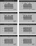
The impedance calculation is generally performed using the Polar SI9000 impedance calculation tool. Common impedance models need to be known before calculations. Common impedance models include characteristic impedance model, differential impedance model, and coplanar impedance model. As shown in Figure 10-50, impedance models are subdivided into the following categories.
(1) Outer layer characteristic impedance model.
(2) The inner layer characteristic impedance model.
(3) Outer layer differential impedance model.
(4) Inner layer differential impedance model.
(5) Coplanar impedance model.
① Outer layer coplanar characteristic impedance model.
② Coplanar characteristic impedance model of inner layer.
③ Outer layer coplanar differential impedance model.
④ Inner layer coplanar differential impedance model.
Figure 10-50 Common Impedance Models

Detailed Impedance Calculation
1.Necessary Conditions for Impedance Calculation
The necessary conditions for impedance calculation are board thickness, number of layers (signal layers, power supply layers), plate, surface process, impedance value, impedance tolerance, and copper thickness.
2.Factors Affecting Impedance
The factors that affect the impedance include dielectric thickness, dielectric constant, copper thickness, line width, line spacing, and solder mask thickness, as shown in Figure 10-51.

Figure 10-51 Factors Affecting Impedance
In Figure 10-51, H1 is the thickness of the dielectric (PP sheet or sheet, excluding copper thickness); Er1 is the dielectric constant of the PP sheet or sheet, which is the average value when multiple PP sheets or sheets are pressed together; W1 is the line width under the impedance line; W2 is the line width on the impedance line; T1 is the copper thickness of the finished product; CEr is the dielectric constant of the green oil (3.3); C1 is the green oil thickness of the substrate (generally 0.8mil); C2 is the copper Thickness of green oil on leather or traces (usually 0.5mil).

Impedance calculation method
The following is an example to demonstrate the method and steps of impedance calculation.
Ordinary FR-4 sheets generally have sheet suppliers such as Shengyi, Kingboard, and Lianmao. The core board of Shengyi FR-4 and equivalent materials can be divided according to the thickness of the board. Table 10-5 lists common Shengyi FR-4 core board thickness parameters and dielectric constant.
Prepreg (ie PP sheet) generally includes 106, 1080, 2116, 7628 and so on.

Table 10-6 Common PP sheet thickness parameters and dielectric constants

For Rogers sheet, Rogers4350 0.1mm sheet has a dielectric constant of 3.36, other Rogers4350 sheets have a dielectric constant of 3.48; Rogers4003 sheet has a dielectric constant of 3.38; and Rogers4403 prepreg has a dielectric constant of 3.17.
We know that each multi-layer board is formed by pressing the core board and the prepreg. When calculating the laminated structure, it is usually necessary to stack the core board and the PP sheet together to form the thickness of the board. For example, if a core board and two PP sheets are superimposed “core board + 106+2116”, then its theoretical thickness is 0.25mm+0.0513mm+0.1185mm=0.4198mm. But pay attention to the following points.
① Generally, 4 or more PP sheets are not allowed to be stacked together, because the sliding phenomenon is easy to occur when pressing.
②The PP sheet of 7628 is generally not allowed to be placed on the outer layer, because the surface of 7628 is relatively rough, which will affect the appearance of the board.
③ 3 sheets of 1080 are not allowed to be placed on the outer layer, because it is easy to cause slippage when pressing.
④The core board is generally larger than 0.11mm, generally two core boards for 6 layers, and three core boards for 8 layers.
Due to the thickness of copper, there is a certain gap between the theoretical thickness and the measured thickness. For details, please refer to Figure 10-52.

Figure 10-52 Theoretical thickness and measured thickness
It can be seen from Figure 10-52 that there is a difference between the theoretical thickness and the measured thickness of copper thickness, and the following formula can be summarized.
Measured thickness = theoretical thickness – copper thickness 1 (1-X1) – copper thickness 2 (1-X2)
In the formula, X1 and X2 represent the residual copper ratio, which is 1 for the surface layer and 0 for the light plate. The residual copper rate of the power ground plane is generally 70%, and the residual copper rate of the signal layer is generally 23%.
The residual copper rate refers to the ratio of the area of copper on the board plane to the area of the entire board. For example, the residual copper rate of unprocessed raw materials is 100%, and when it is etched into a light plate, it is 0%.
“OZ” means the copper thickness unit “ounce”, 1OZ=0.035mm.
Impedance calculation example
(1) Lamination requirements: the plate thickness is 1.2mm, the plate is FR-4, the number of layers is 6, the inner layer copper thickness is 1OZ, and the surface layer copper thickness is 0.5OZ.
(2) According to the combination of common thickness parameters of core board and PP sheet, and according to the requirements of lamination thickness, the lamination structure shown in Figure 10-53 can be stacked.

Figure 10-53 6-layer stacking structure diagram
The thickness of the PP sheet marked in Figure 10-53 is the actual thickness, and the calculation formula is as follows.
PP (3313)[实测值]=0.1034mm[理论值]-0.035/2mm×(1-1)[表层铜厚为 0.5OZ,残铜率取 1]-0.035mm×(1-0.7)[内层铜厚为 1OZ,残铜率取 70%]=0.0929mm=3.65mil
PP (7628×3)[实测值]=0.1951mm×3[理论值]-0.035mm×(1-0.23)[内层铜厚为 1OZ,相邻信号层残铜率取 0.23%]-0.035mm×(1-0.23)[内层铜厚为 1OZ,相邻信号层残铜率取 0.23%]= 0.5314mm=20.92mil
The total thickness of the board
=0.5OZ+3.65mm+1OZ+5.1mm+1OZ+20.92mm+1OZ+5.1mm+1OZ+3.65mm+0.5OZ= 1.15mm
(3) Open the Polar SI9000 software, select the impedance model whose impedance needs to be calculated, and calculate the 50-ohm single-line impedance line width on the surface layer. As shown in Figure 10-54, according to the lamination data, fill in the relevant known parameters, and calculate the trace width W0=6.8mil. This is to calculate a relatively thick trace, and sometimes there will be a certain error in the allowable impedance based on the difficulty of the trace, so it can be slightly adjusted according to the calculated trace width. For example, when the calculation parameter is adjusted so that the trace width is 5.5mil, the calculated impedance Zo=54.82, as shown in Figure 10-55.

Figure 10-54 Calculating line width from impedance

Figure 10-55 Fine-tuning the impedance value according to the line width
(4) It is necessary to calculate the line width and spacing of the 90-ohm differential impedance traces of the inner layer (taking the third layer as an example), as shown in Figure 10-56, select the differential impedance model of the inner layer, and fill in the After knowing the parameters, you can adjust the line width and spacing according to the impedance requirements, and calculate them separately. Considering the difficulty of the board design, the fine-tuning impedance can be within the allowable range.

Figure 10-56 Calculation result of 90 ohm differential impedance
(5) The final calculation results are shown in Table 10-7.
The Links: LM64N731 EL640.480-AA1

