
“The PCB design is complicated, and various unexpected factors frequently affect the achievement of the overall solution. How can we tame scattered parts with different personalities? How to draw a neat, efficient and reliable PCB diagram? Let’s take a look today.
“
The PCB design is complicated, and various unexpected factors frequently affect the achievement of the overall solution. How can we tame scattered parts with different personalities? How to draw a neat, efficient and reliable PCB diagram? Let’s take a look today.
The PCB design seems complicated. It is necessary to consider the direction of various signals and the transmission of energy. The troubles caused by interference and heat are always with us. But in fact, the summary is very clear, and we can start from two aspects:
To put it more bluntly, it is: “how to place” and “how to connect”.
Does it sound very easy? Let’s first sort out the “how to swing”:
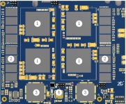
1. Follow the layout principle of “big first, then small, first difficult and then easy”, that is, important unit circuits and core components should be prioritized. This is the same as eating a buffet: if you have a limited appetite in a buffet, choose what you like first, and if you have limited PCB space, choose what you like first.
2. The schematic diagram should be referred to in the layout, and the main components should be arranged according to the flow direction of the main signal of the single board. The layout should meet the following requirements as far as possible: the total wiring is as short as possible, and the key signal lines are the shortest; the layout of the decoupling capacitors should be as close as possible to the power pins of the IC, and the loop formed between them and the power supply and the ground should be the shortest; reduce the signal Run the wrong way to prevent accidents on the road.

First big then small, first difficult then easy
3. The arrangement of components should be convenient for debugging and maintenance, that is, large components cannot be placed around small components, and there should be enough space around the components to be debugged. If it is too crowded, it will often become embarrassing.
4. For the circuit parts of the same structure, the “symmetrical” standard layout should be adopted as much as possible; the layout should be optimized according to the standards of uniform distribution, balanced center of gravity and beautiful layout.
Evenly distributed, balanced center of gravity
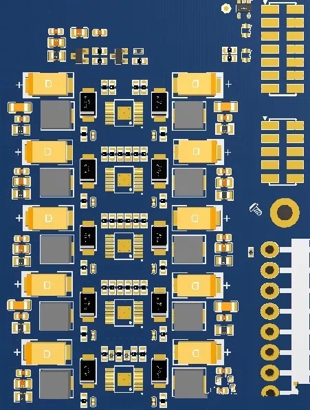
5. The same type of plug-in components should be placed in one direction in the X or Y direction. The same type of polarized discrete components should also strive to be consistent in the X or Y direction, which is convenient for production and inspection.
Uniform Polarity Layout
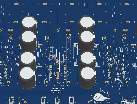
6. Generally, the heating elements should be evenly distributed to facilitate the heat dissipation of the single board and the whole machine. The temperature sensitive devices other than the temperature detection element should be kept away from the components with large heat generation.
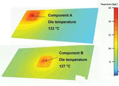
Heat-generating components are evenly distributed
7. High-voltage, high-current signals are completely separated from low-current and low-voltage weak signals; analog signals are separated from digital signals; high-frequency signals are separated from low-frequency signals; the interval between high-frequency components should be sufficient. When laying out components, due consideration should be given to placing devices using the same power supply as close as possible to facilitate future power supply separation.
What are the rules to follow to draw an excellent PCB diagram?
The above are the main points to note about “how to place” or layout. And about “how to connect” is relatively more complicated, generally speaking:
Key signal line priority: priority wiring of key signals such as analog small signal, high-speed signal, clock signal and synchronization signal;
Density priority principle: Start wiring from the device with the most complex connection relationship on the single board. Start routing from the area on the board with the densest connections.
The Links: SKM100GB128DN FZ3600R17KE3_B2 IGBT-CENTER


