
“As cars are equipped with more and more sensors and functions, the amount of electronics in the car continues to increase, and so does the power level. Engineers who have relied on low dropout linear regulators (LDOs) in the past may now need to use a buck topology to meet the high efficiency requirements of their systems.
“
This article is compiled from EDN, by Zachary Imm, TI Automotive Electronics Marketing Manager
As cars are equipped with more and more sensors and functions, the amount of electronics in the car continues to increase, and so does the power level. Engineers who have relied on low dropout linear regulators (LDOs) in the past may now need to use a buck topology to meet the high efficiency requirements of their systems.
A buck can deliver more power than a typical LDO at higher efficiency, but has one significant disadvantage – its switching characteristics generate electromagnetic interference (EMI), which can be a serious problem for automotive applications . Fortunately, engineers can use many tricks and tools to reduce EMI, including optimizing board layout, leveraging IC capabilities, and adding circuitry.
DC/DC converters generate EMI due to input ripple, electromagnetic coupling from nearby circuits, and electromagnetic radiation. EMI can interfere with AM/FM radio receivers and other sensitive equipment, such as the head unit or advanced driver assistance system (ADAS) sensors. Severe EMI can create static or other types of noise in the radio and host audio, interfere with ADAS sensors, and degrade the performance of other systems.
To prevent such severe interference, engineers need to design systems that comply with official standards, such as CISPR 25 Class5. Since poor layout can cause devices to fail the EMI limits set by standards bodies, good layout optimization practices need to be followed during board layout. The most important practices for a buck converter are:
Reduce the surface area of the node by rapidly changing voltage (high dv/dt).
Reduce the area of the current loop with rapidly changing currents (high di/dt).
These two ground rules will dictate where engineers place certain components to minimize EMI.
Unfortunately, even the most optimized PCB layout cannot prevent all EMI-related problems. Furthermore, due to board size, shape or timing constraints, it is often not possible to optimize the layout of EMI as much as possible. For example, a very compact layout might require you to place the power Inductor on the bottom of the board, or place the input capacitor a little further away from the IC.
These and other layout constraints can cause EMI, which can degrade system performance. Even with experience and extreme caution, boards may need further optimization. These additional board revisions take time and money. So what can you do other than optimize the layout to minimize the EMI of the application?
Bypass board layout constraints
If the layout cannot be optimized for optimal EMI, some DC/DC converters offer many packaging and functional improvements at the device level to help minimize EMI and make it easier to meet CISPR 25 Class5 limits. These features make board design independent of layout. In other words, they can help make up for layout flaws.
For example, spread spectrum is a function that spreads harmonic energy to reduce peak and average EMI measurements. By modulating the peak clock to change it from a narrowband clock to a spectrum with sidebands, the peak energy is dispersed to multiple frequency bands in the spread spectrum region, thereby reducing the peak energy and suppressing EMI. It spreads the spectral density by dithering the switching frequency, e.g. by ±2%, will see the harmonic energies fully mixed or overlapped at the 25th and higher harmonics instead of a fixed frequency, which will keep the harmonic spike at the fundamental frequency. The energy is evenly distributed in the higher frequencies, resulting in a lower measured value envelope, requiring less filtering and less layout optimization, saving time and money.
Slew rate control is another feature that helps improve EMI performance, the main source of EMI being the switching loop. The switching loop is caused by the fast turn-on of the high-side FET, which rapidly pulls current from the input capacitor, the resonance of the input parasitic loop inductance and the parasitic capacitance of the low-side FET, and can generate hundreds of megahertz of ringing noise. By slowing the rise time will slow down the current consumption, thus reducing ringing and EMI. The rise time can be slowed down by adding a resistor (on the order of a few ohms) in series with the boot capacitor, and some devices have a dedicated boot resistor pin. There is a trade-off here: slowing down the FET minimizes EMI, but also increases switching losses, which reduces efficiency.
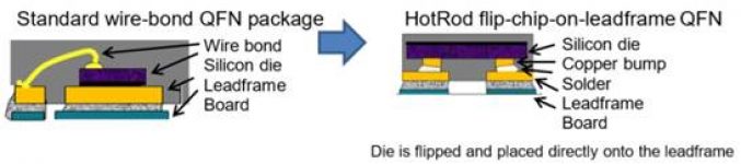
In addition, there are some packaging techniques that help suppress EMI. One example is TI’s HotRod package, which eliminates internal bond wires, as shown in Figure 1. Discontinuous current flow can cause hundreds of megahertz of ringing on the switch node, which can couple and radiate, causing EMI. Removing the bond wire in the high di/dt loop path of the input capacitor discontinuous current reduces the loop inductance. This reduces ringing and reduces EMI. The HotRod family of products includes devices such as the LM61460-Q1 and LM53635-Q1.
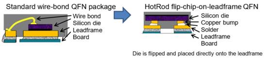
Figure 1 The difference between standard QFN and TI’s HotRod QFN.Source: Texas Instruments
Other package-level features include optimized pinouts. Devices can improve EMI performance by trimming pin locations so that critical paths, such as input capacitors, are kept as small as possible. Devices typically place the VIN and GND (or PGND) pins next to each other to provide the best location for capacitor connections.
Going a step further, a symmetrical pinout is used. Placing VIN/PGND symmetrically on either side of the package allows the input loop magnetic field to self-contain, further reducing EMI. Many DC/DC buck converters, such as the LMR33630, LMR36015, LM61460, and LMQ61460-Q1 have symmetrical VIN/PGND pin pairs (Figure 2b).
Integrated input capacitor
Next-generation products in EMI-optimized packages employ integrated capacitors to further reduce input parasitic inductance. Each side of the LMQ61460-Q1 contains two integrated input bypass capacitors, one for each VIN/PGND pair. These capacitors are the dark rectangles that span the upper and lower right pin pairs (VIN and PGND) shown in Figure 2a. Figure 2b shows the pinout of the device for reference.
Minimizing high-frequency EMI is especially important because the higher input voltages and higher output currents commonly found in automotive applications can exacerbate problems in this area.
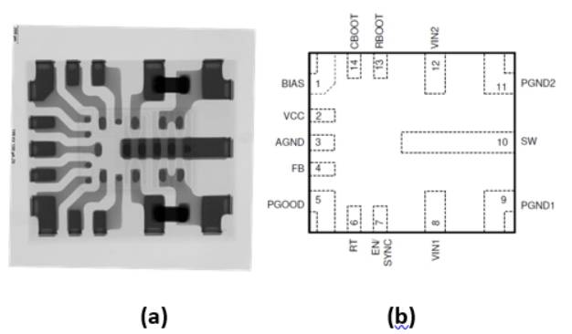
Figure 2 shows the LMQ61460-Q1 step-down low noise converter with integrated capacitors (a) using X-rays (which can be referenced to pins (b)).Source: Texas Instruments
It’s true that EMI presents challenges in automotive applications, but design engineers are not out of options if they encounter board layout constraints. From strategic device pinouts to integrated features such as low-inductance packaging, slew rate control, spread spectrum, and integrated capacitors, there are many ways to address this challenge.
These features allow engineers to relax strict optimization of EMI layout in exchange for a more comprehensive layout design, leaving more room for optimized performance for better thermal performance and/or smaller solution size. These features improve your designs to meet EMI limits set by standards bodies with confidence.
The Links: LQ190E1LW42 EVK71-060


